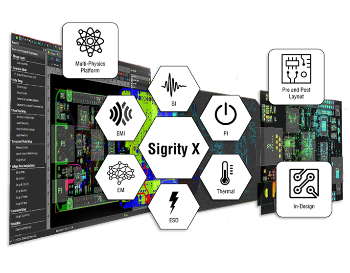
Solve The Next Generation of Design Challenges with Sigrity X
If you hope to stay ahead of the competition, you must determine optimal design configurations, validate performance, and signoff on your critical interconnects well before you get to prototype. Sigrity X provides the only complete analysis solution designed to solve today’s multi-physics, multi-domain design challenges.
Sigrity allows you to move to production with confidence by providing a complete sign-off level design, analysis, and compliance environment for your critical serial link and parallel bus interfaces.
Simulate Anything, Anywhere, Anytime With Sigrity X
Sigrity X Signal Integrity
Sigrity X Signal Integrity
Key Sigrity SI Capabilities
Serial Link Analysis (PCIe, USB, etc.)
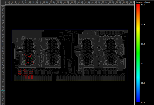
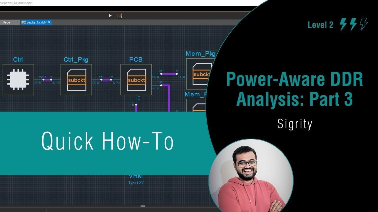
Power-Aware Parallel Bus Analysis (DDR)
Interface Sign Off with Pass/Fail Compliance Analysis
Pre-Layout and Post-Layout Analysis
Automated Reporting
Wizard-based Workflows
Key Sigrity SI Capabilities
Serial Link Analysis (PCIe, USB, etc.)
Power-Aware Parallel Bus Analysis (DDR)
Interface Sign Off with Pass/Fail Compliance Analysis
Pre-Layout and Post-Layout Analysis
Automated Reporting
Wizard-based Workflows
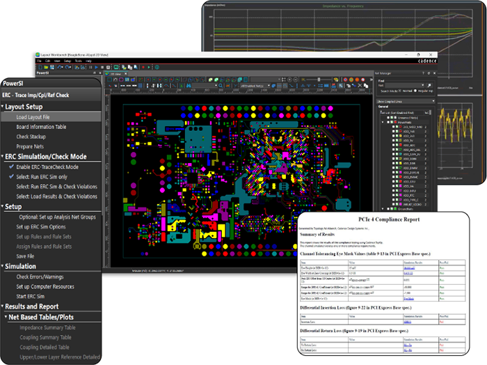
Comprehensive Signal Integrity Analysis
Achieve comprehensive electrical analysis of PCB and full IC packages with accurate, power-aware pre-layout and post-layout simulation to improve signal quality and performance.
Available Workflows
Impedance Reflection Coupling Crosstalk Return Path Power Ground Noise TDR/TDT Serial Link Analysis Parallel Bus Analysis Channel S-Parameter Model Extraction
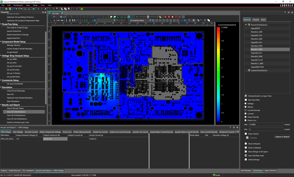
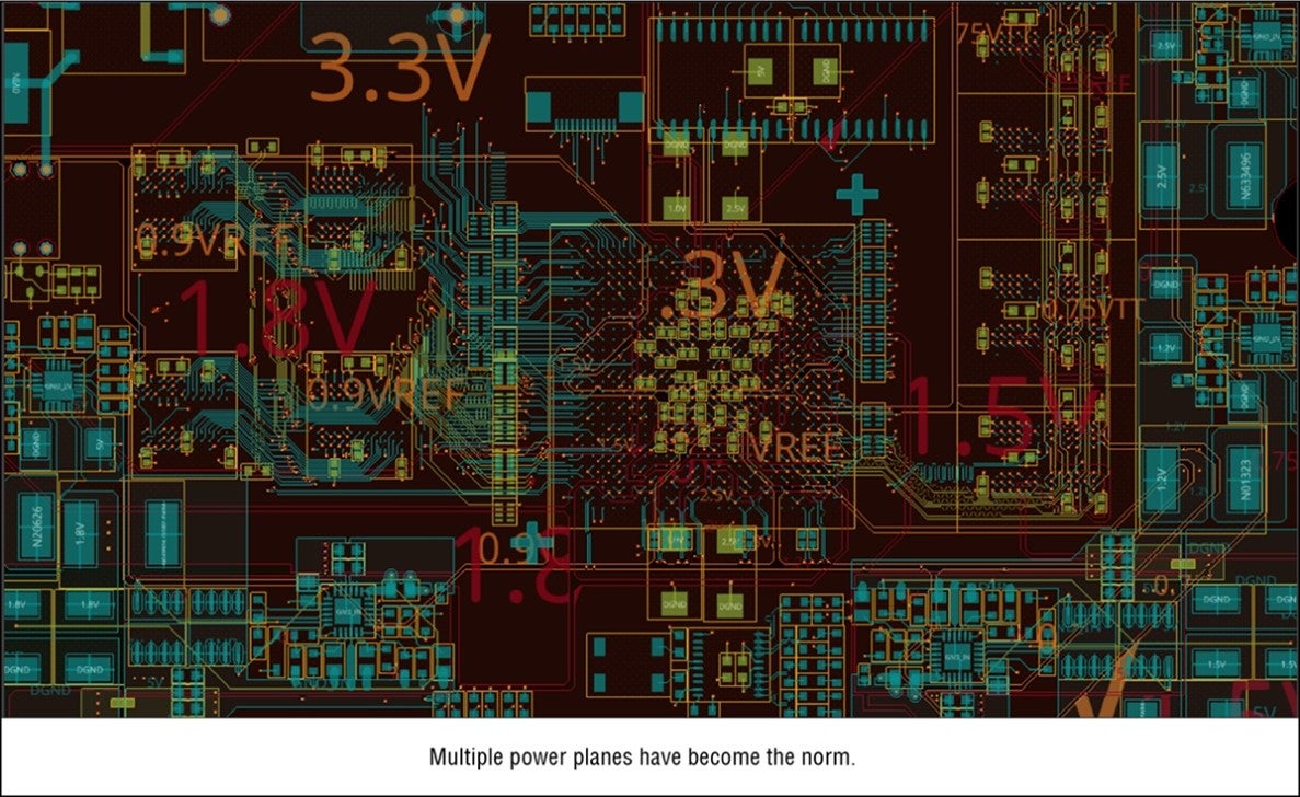
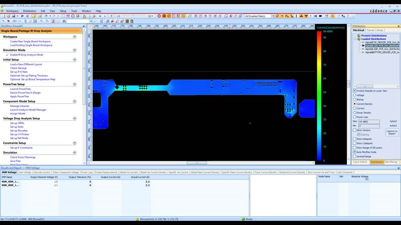
Power Delivery Network (PDN) Analysis and Optimization
Decoupling Capacitor Optimization
Pre-Layout and Post-Layout Analysis
Automated Reporting
Wizard-based Workflows
Key Sigrity PI Capabilities
Power Delivery Network (PDN) Analysis and Optimization
Decoupling Capacitor Optimization
Pre-Layout and Post-Layout Analysis
Automated Reporting
Wizard-based Workflows
Comprehensive Power Integrity Analysis
Analyze and optimize your Power Delivery Network (PDN) using AC frequency analysis as well as pre-layout and post-layout simulations to adhere to PDN requirements at the lowest possible cost.
Available Workflows
IR Drop Resistance Measurement Resistance Generation PDN Impedance Checking Capacitor to IC Device Loop Inductance IC Device Power Pin Inductance Best Capacitor Location Estimation Decoupling Cap Optimization Pin Location Effectiveness Resonance Noise Coupling PDN S-Parameter Model Extraction
Adaptive mesh refinement for IC package and PCB designs
Accurate EM solutions for ECAD/MCAD 3D structures
Low Memory Footprint, Near Linear Scalability
Parallelization & Cloud-scaling ready
Key Sigrity EM Capabilities
Multi-solver (2D, 2.5D, 3D, MoM, Q3D, FDTD)
S-parameter Characterization & Analysis
Adaptive mesh refinement for IC package and PCB designs
Accurate EM solutions for ECAD/MCAD 3D structures
Low Memory Footprint, Near Linear Scalability
Parallelization & Cloud-scaling ready
Electromagnetic Analysis Built for Accuracy, Performance, and Capacity
Sigrity X EM analysis solutions are built for accuracy and speed enabling you to simulate your increasingly complex structures without compromise. With a 10x performance increase over the competition you can be assured you will be able to simulate with the fidelity you need and the speed you want. Multiple solver engines enable designers to leverage the best solver for the task (or deploy a combination) all from a cohesive and intuitive user interface.
Available Workflows
3D Layout Full-Wave Spatial 2.5D Multi-Board Power-Aware Model Extraction Package Extraction
Evaluate near-field E/H densities and radiation effects
Identify problematic EMI radiating devices
Determine necessary shielding and faraday cage placement
Determine the impact of external radiation and system susceptibility
Key Sigrity EMI/EMC Capabilities
Evaluate near-field E/H densities and radiation effects
Identify problematic EMI radiating devices
Determine necessary shielding and faraday cage placement
Determine the impact of external radiation and system susceptibility
Comprehensive EMI/EMC Analysis
Analyze near-field E/H densities and radiation effects as well as the impact of external radiation to easily identify problematic EMI radiating devices, determine necessary shielding and faraday cage placement, and evaluate overall system susceptibility.
Available Workflows
EMC/EMI Simulation Plane Wave Susceptibility S-Parameter Model Extraction
Incorporation of External Heat Sources and Thermal Transfer Coefficients
FEM Solver for Accurate Conductive Joule Heating Analysis
Powerful Computational Engine and Meshing Technology
Key Sigrity Thermal Capabilities
Full System Electrothermal Co-Simulation
DC Static and Transient Analysis
Incorporation of External Heat Sources and Thermal Transfer Coefficients
FEM Solver for Accurate Conductive Joule Heating Analysis
Powerful Computational Engine and Meshing Technology
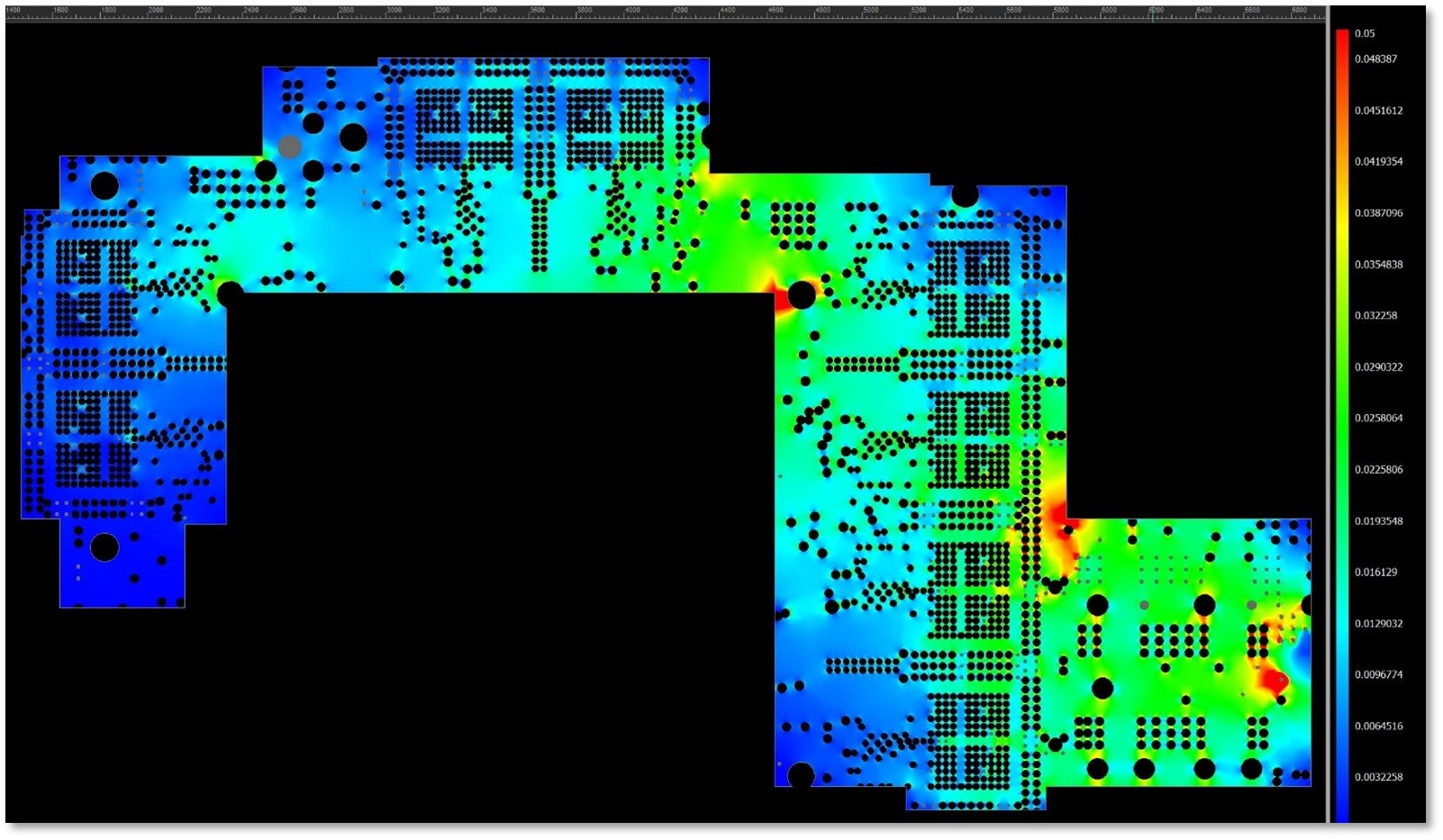
Comprehensive Thermal Analysis
Heat is one of the biggest factors in the performance, reliability, and safety of your PCB designs. Thermal effects can be simulated and heat mitigation efforts can be incorporated within your electronics early using Sigrity X. Efficiently identify hotspots and optimize your thermal profile as you design to ensure products will stay cool and function as intended.
Realistic Representation of IEC-61000-4-2 Testbench Environment
Emulate ESD Pulse Injections
Analyze the Effects of a Physical ESD Gun on Your Design
Key Sigrity ESD Capabilities
Realistic Representation of IEC-61000-4-2 Testbench Environment
Emulate ESD Pulse Injections
Analyze the Effects of a Physical ESD Gun on Your Design
Comprehensive ESD Analysis
Emulate and analyze the effects of a physical ESD gun on the design to prevent product damage, ensure adherence to regulatory standards and improve reliability.
Connected with the tools and formats you work with every day
The Sigrity Difference
Unmatched Ease of Use
Unified Design Environment
The unique, workflow-driven design environment and comprehensive simulation engines allow you to quickly access and perform the analysis needed to meet your design goals. As your analysis requirements increase, easily add additional workflows all within the same common UI. Never miss a step or feel unsure of your simulation setup with Sigrity workflow driven analysis.
Workflows Step-by-step analysis processes
The unique, workflow-driven design environment and comprehensive simulation engines allow you to quickly access and perform the analysis needed to meet your design goals. As your analysis requirements increase, easily add additional workflows all within the same common UI. Never miss a step or feel unsure of your simulation setup with Sigrity workflow driven analysis.
Multi-CAD CAD neutral by design
Perform comprehensive analysis of your PCBs regardless of the file format or CAD tool used for the design. Sigrity X accepts neutral file formats, such as IPC-2581 and ODB++, as well as CAD-specific files such as Altium, Cadence, Mentor, and Zuken.
PCB & IC PKG Aware
Automate simulation prep and setup
Drastically reduce simulation setup time and errors with PCB & IC PKG aware setup with Sigrity X. Sigrity X understands PCB & Package structures and natively integrates with the Cadence PCB file formats to automate port configurations and make flex and rigid-flex simulation setup easy and straightforward.
Automated Reporting Easily capture and share simulation results
Automatically generate reports containing tabular data, plots, pass/fail results, and more to efficiently communicate the analysis and required changes for your PCB designs.
Uncompromising Analysis At All Stages
Shift Left With Sigrity X
Simulation shouldn’t be a singular event for the end of the design. To maximize the benefit and effectiveness of simulation in your design flow it is important to be able to simulate effectively at any stage. Sigrity X provides access to the most comprehensive range of simulation engines and tools to allow for full multi-physics analysis to occur at all phases enabling a true simulation driven digital twin-based design flow.
Sigrity Tokens Flexible and cost effective access
Gain access to the full Sigrity X platform on-demand with Sigrity tokens. Sigrity tokens solves one of the most prevalent problems for teams looking to adopt a simulation-driven workflow, usage and solver access. Traditional models require purchase of each solver and analysis tool separately with many of the tools sitting idle while those particular simulation engines are not needed. This makes justifying the cost of simulation tools a big challenge and leaves you susceptible to other SI/PI issues that cannot be analyzed. Sigrity tokens allows teams to leverage the full Sigrity X portfolio on-demand saving significant costs and enabling simulation to be broadly used throughout the design process, ensuring high utilization and efficiency.
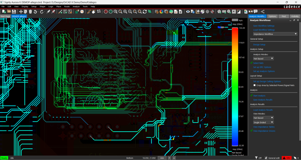
In-Design Analysis Simulate and fix direclty inside your PCB design environment
Analyze common SI and PI problems without leaving your PCB design environment. Graphical overlays as well as tabular results help you easily identify and correct issues directly in the PCB canvas as you design.
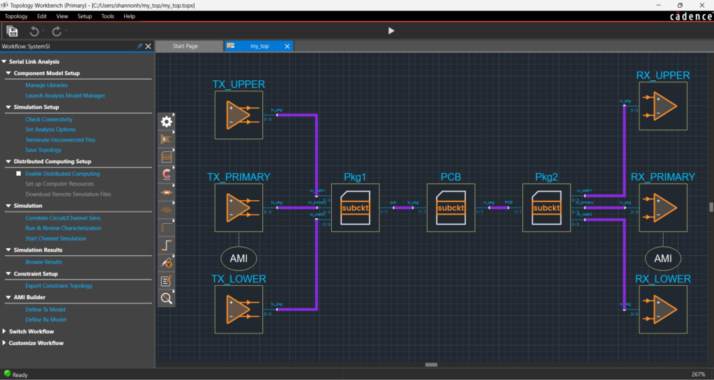
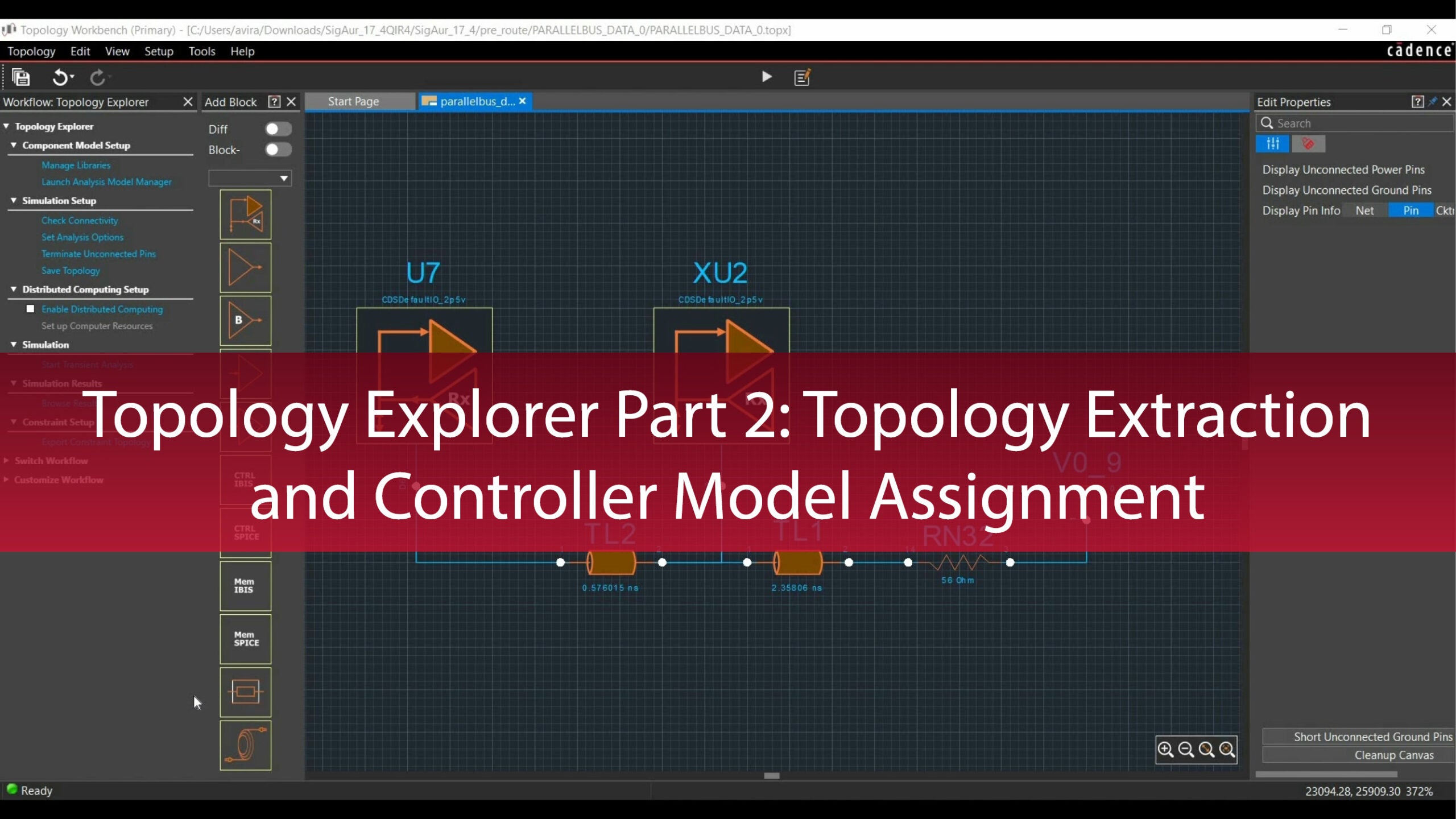
Topology Workbench Powerful pre and post layout analysis & optimization
TopXP provides a ready-made interface for pre and post layout exploration and analysis. From single board to multi-board system level simulation, TopXP provides the flexible easy-to-use environment needed to perform your SI/PI analysis.
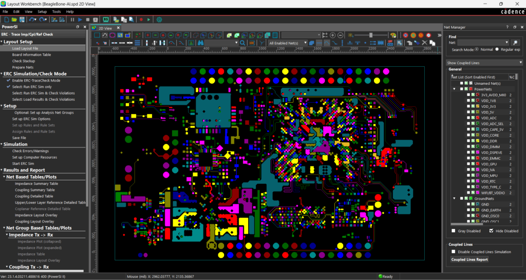
Layout Workbench Full board multi-physics analysis
Interact with the physical design and run full board simulation and extraction to build models and test your design effectiveness. Perform multi-corner optimization, such as decap placement, with ease.
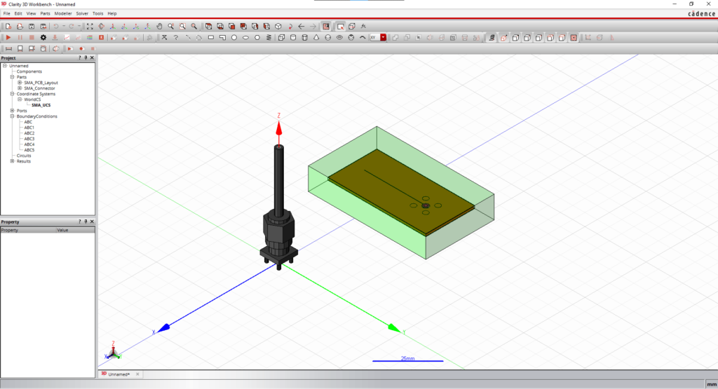
3D Workbench Full Wave 3D electrical and mechanical simulation
Easily and model your complex 3D structures from via, to connectors, and full flex PCBs. With automated setup and unmatched performance, you can ensure hardware correlated accuracy for your critical 3D structures.
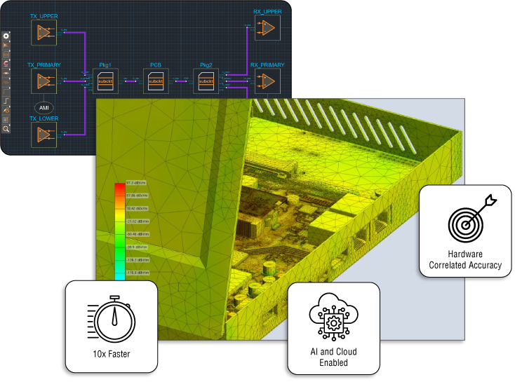
Industry Leading Performance, Capacity, & Accuracy
Build True Virtual Prototypes
Often the size and granularity of simulations required to obtain a real-world analysis results in lengthy run times that are not feasible in today’s fast-paced markets. Sigrity X allows you to build true virtual prototypes and perform analysis quickly with the industry leading performance, capacity, and accuracy.
Parallelized Architecture 10x your simulation performance
Full multi-threading support allows you to accelerate analysis speed even farther by leveraging your multi-core compute resources to go from run to results in no-time.
Cloud Accelerated Scale seamlessly and linearly
Easily leverage the cloud to scale your compute resources with near linear improvement in performance. With the lowest memory footprint on the market, you can scale cost effectively levering less expensive compute resources while producing faster results.
Full 3D Signoff High capacity high accuracy 3D EM
Clarity 3D EM was architected from the ground up and provides the fastest, highest capacity, lowest memory footprint solution for EM extraction. Simulate with confidence knowing that you can handle the most complex solution spaces without approximation or cut and stitch, ensuring what you analyze represents what you will build.
Hardware Correlated Simulate what you build
Analyze and verify with confidence knowing your results will have tight correlation to real-world hardware. Cadence rigorously tests Sigrity X against their own hardware ensuring the correlation you need to sign-off with confidence.
Optimize with AI AI-Assisted design exploration
AI-powered optimization architecture enables efficient evaluation of design corners and design alternatives to perform hardware-accurate system-level optimization in a fraction of the time based on defined design goals.
Sigrity X Courses
Training Included
Access free training materials from EMA and Cadence to get you simulating with maximum efficiency right from the start.
Sigrity X allows PCB designers, electrical engineers, and SI experts can now edit and analyze designs in parallel , freeing the design team to rapidly move through multiple design phases and avoid separate out-of-sync design files reducing the amount of time required for each PCB design.
Bob FreySenior Director SMART Modular Technologies
IAC is committed to R&D and manufacturing smart terminal products in various fields. The Cadence Sigrity X and Clarity 3D Solver technologies have excellent performance and accuracy, which help us find and solve SI/PI problems early in the design process for our smart wearable devices.
LI ZHIYONGDevelopment Manager IAC Engineering
Finally, A Simulation Solution for Everyone
From single users to large teams Sigrity X enables you to leverage simulation at all phases.
Sigrity X for Electrical Engineers
Get access to the easy-to-use comprehensive simulation environment which allows you to run analysis quickly and accurately across SI, PI, Thermal and more.
Sigrity provides the fastest, highest capacity simulation environment available. Expert level users need expert level tools that can support the complex design challenges you are faced with. Sigrity represents the most advanced electronics multi-physics simulation platform available on the market.
Up to 10x faster run-times than other leading simulation engines
Accurate, hardware-correlated results
Automated reporting
Unified Design Environment for all your SI/PI/EMC needs
Multi-Physics, Multi-Domain Analysis
Sigrity X for PCB Designers
Sigrity X provides integrated in-design analysis allowing you to run simulations as you design. Save time, prevent errors, and leverage simulation to improve your design efficiency with the first simulation environment built to work inside the existing PCB design flow.
Future proof your design team with access to the leading multi-physics analysis platform on the market. Enable your team with the tools they need to identify and solve any electrical analysis issue upfront through simulation. The unique Sigrity X token-based licensing model provides easy access to all the simulation tools and allows you to effectively bring simulation to all users without heavy licenses and access costs. Bring your design predictability, performance, and accuracy to new heights with Sigrity X.