Cadence OrCAD is a driving force in the PCB design industry. In order to help designers keep up with the constant pace of change Cadence has been accelerating the pace of innovation delivering a stream of updates and product enhancements to users. The release history below provides insight into industry-first capabilities made available to customers such as real-time design, DesignTrue DFM, constraint manager, in-design analysis, and more.
Real-Time Interactive 3D Design
See how interactive 3D in OrCAD helps you design in real time with greater accuracy.
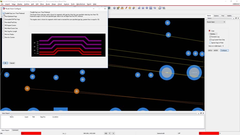
Real-Time Route Analysis
Real-time interactive checks help you easily find and fix common route quality issues that manufacturing DRC signoff checks miss.
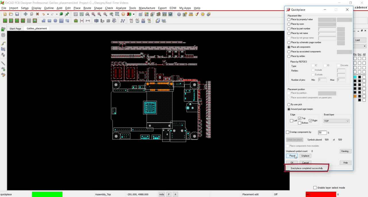
Real-Time Placement Analysis
Visual indicators of length constraints help you meet delay propagation and total etch length goals when placing components.
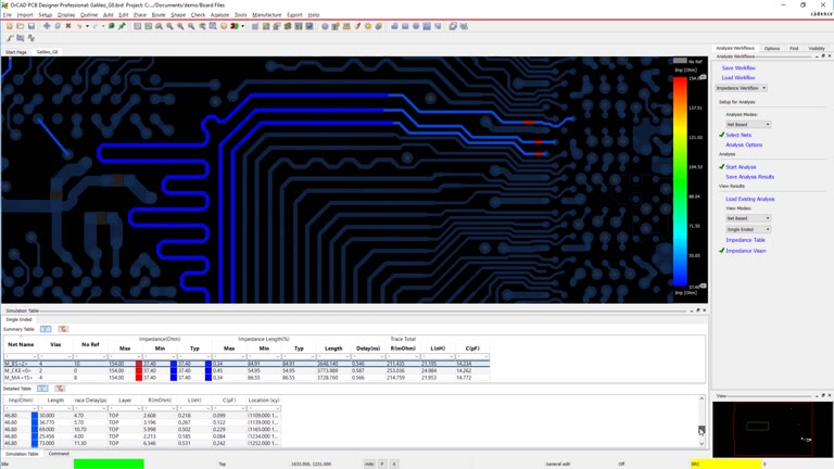
Real-Time Impedance Analysis
Easily and quickly identify impedance discontinuity issues visually, without simulation models or extensive signal integrity expertise.
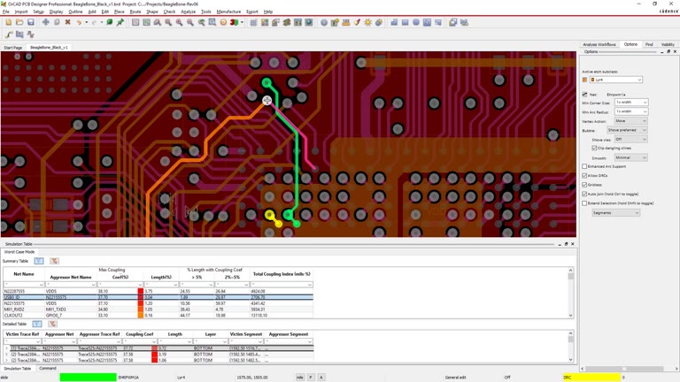
Real-Time Coupling Analysis
Easily and quickly identify coupling issues without always having to rely on the SI expert.
Real-Time Manufacturing Checks
Break out of the find, fix, reiterate cycle with over 200 configurable real-time design for manufacturing checks and get your design right the first time.
Version Notes:
Products Covered: OrCAD X Capture CIS | OrCAD X PCB Editor| OrCAD X Presto | PSpice
ASME 2 level Revision Scheme Support. Automatic ASME 2 level alphanumeric revision scheme within cloud workspaces.
LiveBOM Cross-probe. Cross-probe between LiveBOM and the schematic to efficiently identify at-risk components in the design. OrCAD-X Pro
LiveBOM On Premise CIS Support. Connect to on premise CIS database within LiveBOM to analyze supply chain risk for CIS database components in your schematic designs. OrCAD-X Pro
LiveBOM Enhancements. Enhancements to LiveBOM and ease of use with the inclusion of supply chain lead time and customizable property columns. OrCAD-X Pro
Design Review and Markup Improvements. Easily archive and remove embedded comments to share the design with external users and partners.
3D Enhancements. 3DX canvas has been improved in both OrCAD X PCB Editor and OrCAD X Presto to include cutting planes, material colors, transparency control for all 3D objects, 3D DRC display options, and measuring in 3D.
Object Visibility Improvements. Incorporate stipple patterns for improved object visibility. User-defined views allow you to save views and recall the visibility display in OrCAD X Presto.
Footprint Enhancements. Updates to editing footprints including mass editing of pin locations through the search panel, pad preview in search, and DXF import for footprints.
Paste Special Improvements. Preserve the location of copied shapes for easy replication.
LiveDoc Enhancements. Dimension improvements including alternate units and user-controlled text, panning and zooming improvements, ISO and ASME page sizes, and definition of export PDF location.
ISO Transient Sources. ISO Transient sources for automotive applications including ISO 7637-2 for electrical disturbances form conduction and coupling and ISO 16750-2 for environmental conditions and related testing.
Performance Improvements. Parallel simulation support for parametric sweep, temperature sweep, and Monte Carlo Analysis on desktop to improve performance.
Noise Contributors. Control noise contributors in noise analysis to produce an accurate simulation.
Audio Simulation Support. Use a .wav file as a simulation input or export a .wav file as an output to perform audio simulations.
Simulation Personas. Use and create PSpice simulation personas as a simplified way to globally apply simulator options.
Products Covered: OrCAD X Capture CIS | OrCAD X PCB Editor| OrCAD X Presto | PSpice
OrCAD X Release. Innovative design platform focusing on providing a cohesive and comprehensive solution for all design requirements.
Products Covered: OrCAD Capture | OrCAD PCB Editor| PSpice
Products Covered: OrCAD Capture | OrCAD PCB Editor | PSpice
GPU Acceleration Rendering. Leverage GPU in Allegro Layout Editors to improve response time during panning and zooming, toggling layers, and render quality.
DRC Browser Updates. Navigation improvements for the DRC Browser and the ability to waive DRC by group select.
Fillet DRC Control. New analysis mode option to enable line based checks for fillets.
Shape Performance and Quality Updates. Improved shape performance for copper pours and editing smooth shapes. Fast mode replaces rough mode and drastically improves the performance during active etch editing including slide, add connect, move, and more. Improved performance in shape voiding quality including crosshatch shape fill improvement, fillet void quality improvement, and trim void improvement.
3D Canvas Updates. Isometric view has been added for the bottom side of the board. Other updates include realistic plating thickness, increased model realism, and secondary model support.
Reuse Module Enhancement. Dynamic shapes are automatically converted to static shapes to ensure consistent voiding. Modules applied to the design remain locked to avoid accidental modification. Addition of copper planes, constraint regions and text notes within the module file. Quickly swap a placed reuse module with a different variant in one or multiple locations.
Scribble Enhancements. Multi-pin scribble support when routing allows you to digitize a path through a pin field to make connections. Recognizes the same net pins and snaps to center while routing.
Viewer Integration. Launch PCB Editor viewer from the project hierarchy.
3D Canvas enhancements. 3D mapper now a part of 3D canvas, replacing Allegro (2D) menu. Simplified use model and GUI enhancements. Improved accuracy of collision detection and distance measurements. Additional support for mapping native CAD models (Parasolid, Siemens NX, CREO, SOLIDWORKS).
IPC2581 enhancements. Additional support for rigid flex (bend detail and stack-up profiles), Countersink/counterbore, square drill features, net shorts, and impedance specifications and nets.
IDX enhancements. Bend sequence ordering, Geometry use identification, primary pin identification, and time stamps.
PCB Panelization. Setup and manage your fabrication panels directly within PCB Editor (OrCAD Pro & Allegro Feature).
New Design Setup Workflow. You can now use the new Design Setup Workflow to prepare for analysis by setting up your design for the different checks. You can set up cross-section, DC nets, components, Xnets, and differential pairs. You can then save the design with the changes. As with all other work flows, you can access this workflow from the Analysis Workflows pane (Analyze – Workflow Manager).
3D Canvas Updates. A number of improvements and enhancements have been made to the 3D canvas including:
IPC 2581 Spec Properties. By defining a SPEC that is composed of the fabrication notes, the notes become part of the IPC-2581 data and are directly read by an IPC-2581 viewing tool, reducing the need to locate the correct drawing or document to read the notes. Another example would be to define assembly notes for a heat sink to be added to a part. The assembly note might instruct users to add a specific thermal epoxy first, then add the heatsink after the epoxy is applied.
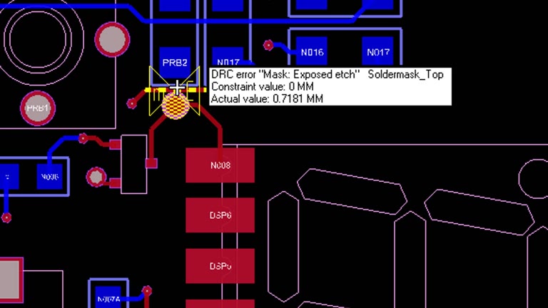
Mask Defined Pin Annular Ring Check. A new Mask Defined Pad check has been added to the Design for Manufacturing Annular Ring checks and the DesignTrue DFM Wizard template file. There are two common types of padstack definitions when it comes to soldermask to pin pad size ratios. The first, metal-defined padstack (sometimes referred to as non-mask defined padstack), is where the solder mask opening is typically larger than the pin pad. The other is a mask-defined padstack, where the solder mask size is typically smaller than the pin pad. The mask-defined pad is often used for BGA components to contain the solder ball within the pin pad and prevent outflow of solder.
Hierarchical Route and Via Keepouts. You can now define keepout by layer type and location using the additional Route and Via Keepout subclasses that have been added to Symbol Editor. Following a model similar to Constraint Regions, use the OUTER_LAYERS, INNER_SIGNAL_LAYERS, and INNER_PLANE_LAYERS subclasses to create keepout shapes.
Contour Routing Update. The 17.4-2019 release now supports the previous Enhanced Contour behavior as the default contouring method. In addition to the previously supported functionality of latching/unlatching and shoving, this release focuses on ease of use and power by adding additional spacing controls and full constraint region support.
Copy/Paste Update. In previous versions of layout editors, copying of objects was performed by selecting objects and pasting them to one location at a time. While the use model was simple, the functionality was limited. The 17.4-2019 release aligns the copying functionality of the layout editors with other popular software applications by adding familiar behaviors. This new copy command combines the precision of single click or single location pasting with the power of window select or multi-location pasting. As with most applications, copied objects are buffered for pasting at a later time. You can paste the last copied object at any time simply by using the paste command.
Copy. The Copy command now adds the selected objects to a buffer and automatically starts the Paste command to enable the placing of objects on the canvas.
Paste. The Paste command supports all legacy “copy” options as well as new support for shape net retention. In addition to these options, pasting can be used in two different manners:
3DMechanical Symbol Transparency. Designers who wish to “peek” inside a PCB assembly encased with a mechanical cover can now do so. Now look through the mechanical cover into an assembly by setting the global transparency/opaqueness setting.
Unplated Holes in Footprints. Unplated holes in footprint (.dra) files can now be visualized when the footprint is brought into 3D Canvas. Previously, unplated holes were not represented.
STEP Models and Pastemask. In some system designs, such as complicated telephony devices, even the most minuscule space is critical. With the 17.4-2019 release, the position of 3D models can now be globally adjusted to take the thickness of solderpaste into account in the “z” direction. By default, the STEP model location in the “z” direction is the bottom of the model located directly on top of the copper pads.
Access to TI Libraries. Access additional Texas Instrument Libraries from OrCAD Capture including 5000 TI-PSpice Models across 100 unique model categories and as many as 4000 test circuits.
Improved Usability. Auto launch of PSpice on new project creation, updated menus, and updated PSpice search.
MATLAB 2020/2021 Support. MATLAB 2020/2021 support is now available for PSpice co-simulation flows.
Usability updates. Get notified for missing parts for your PSpice models as you place them with Online DRC. Navigate warnings and errors with cross-probe between DRC and schematic. PSpice parts are loaded automatically when a new PSpice project is created. Improved capture integration with the ability to view PSpice models within Capture.
New modelling applications. Easy-to-use DIODE and MOSFET model parameters from device datasheet, specifically targeted for power applications.
Products Covered: OrCAD Capture | OrCAD PCB Editor| PSpice
Enhancements in Part Editor. With QIR 7, you will see the following enhancements in part editor:
Simplified Interface for Associating a PSpice Model. You can now accomplish the following tasks to associate a PSpice model using a simplified user interface:
Performance Improvement. Performance has been improved for various design specific cases, such as designs with large number of netgroups.
Design View in HTML. This new feature allows you to export a complete schematic design as a single HTML file, and view the design in the specified internet browser (Google Chrome recommended).
Saving Design Differences to HTML or Excel. OrCAD® Capture Design Differences Viewer now supports the ability to save the design differences into HTML files (.html) or Excel files (.xls).
Passport Protection to a Design in Capture. You can now add a password to a design, remove an existing password applied to a design, or modify an existing password applied to a design.
Configuring Properties. You can configure the Find window properties and Browse Parts window properties using the Configure Properties window.
New Utilities. New utilities have been added in OrCAD Capture to automate some of the manual tasks, including: Communication Server, Replace Path in Design Cache, Show All Open Libraries and Design, Customize Page, Check/Correct Corrupt Library, and Find and Replace Text.
Display Checkbox in Add New Property Dialog. Enable display of user-defined properties so that you can set display properties while creating a new user-defined property.
Updated Property Editor Filter in the Properties Editor Window. Updated and flow-wise property spreadsheet filters are now available, so you don’t need to search for commonly used properties for a flow.
Global DRC Settings for Global Environments. A new option, Use Global DRC Settings, has been added in the DRC tab of the Extended Preferences Setup window. By enabling this option, you can use the same DRC settings globally for various different designs to enable standardization of a DRC setting across projects, sites, and teams
Design Difference Viewer. New feature to perform logical and graphical comparisons between two designs, two schematic folders or two schematic pages and view the difference report in the form of a portable HTML format. (Watch Demo Video)
Open Demo Design. The new Open Demo Design browser gives access to more than 150 demo designs made available from different locations, collated together to help users better understand Capture, Capture CIS and Capture _ PSpice Flow.
Export – Import XML. OrCAD Capture provides you the capability to convert Capture designs to XML format and vise-versa based on the requirement.
ISCF Export. Introducing direct ISCF (Intel Schematic Connectivity Format) feature for automating Intel-based design reviews to export hierarchical schematic designs in an Intel-approved format helping you optimize the design review process.
PDF Export. The new PDF export functionality lets you export Capture design as PDF file and provides intelligent design information.
Extended Preferences setup. The extended Preferences Setup window allows you to modify additional application settings in OrCAD Capture like Command Shell, design and libraries, design rule check, CIS, NetGroup, NetList, and Schematic.
Advanced Annotation. The new advanced annotation feature lets you annotate multiple schematic pages at a time giving them complete control over their component annotation process in the design cycle. (Watch Demo Video)
Design for Fabrication Rule Enhancements. In the Design for Fabrication constraints, a new category Copper Features has been added in this release. This category applies rule to cover minimum line width, antenna, and acid traps.
Design for Assembly Rule Enhancements. A new category PkgToPkg Spacing has been added in the Design for Assembly constraints. You can now maintain the DFA table within Constraint Manager and assign different DFA rules based on stack up technology, specifically within rigid-flex designs. All existing functionalities are still maintained from previous versions.
Design for Testability Rule Enhancements. A new Design for Test constraints have been added in the Manufacturing category in the QIR 7 release. These group of checks are related to issues in the final testing of the PCB assembly.
DesignTrue DFM Ecosystem. To make designs ready for fabrication, the information about various manufacturing constraints and rules and the supported values are obtained from PCB fabricators in the form of spreadsheets. The spreadsheet is then transferred into Constraint Manager by a PCB designer. This process is error-prone and time consuming. The easiest way to obtain the rules would be in the form of direct import of fabricator rules into the Constraint Manager using technology files recognized by Constraint Manager.
DesignTrue DFM Web-Based Rules Request. The DesignTrue DFM Partner Program was developed to facilitate the request for fabrication rules directly from the supplier and receive those rules in the constraint technology file format. You can then directly import the rule files received into Constraint Manager.
To request rules, open the request login site from a Web browser at https:\\pcb.cadence.com\dfm_customer.
3D Canvas Update. The recently productized 3D Canvas continues its growth and maturity with the QIR7 release. With additional features still under development, this release covers incremental updates that will enhance the user experience.
Selecting a specific area of a design to visualize in 3D is now easier with “window select” on the 2D workspace
The popular Cutting Plane feature has been supplemented with a “reverse cutting plane” option
The original Perspective View has been paired with an additional Orthographic View choice
The 3D Canvas now recognizes STEP model colors assigned in the STEP Package Mapper
Color Theme layers now have transparency control sliders and objects falling within holes
Cutouts and outside the board outline are now eliminated from view
Place Vision. Place Vision, available in PCB Editor, is a graphical environment designed to increase productivity and efficiency with various component placement strategies. While the concept is similar to Timing Vision, Place Vision offers guidance with respect to:
Xnet rat filtering
Timing driven Placement
Component Association
Sigrity Technology Driven High-Speed Signal Analysis and Checking. OrCAD® Integrated Analysis and Checking is a new, unique environment blending the best of OrCAD® and Sigrity™ technologies that provides analysis and checking capability entirely within the PCB Editor framework. For rule checking, DRC and ERC capabilities continue to depend on Constraint Manager as the single cockpit. This release introduces two new workflow analysis capabilities for impedance and coupling. The workflows provide guided access to Sigrity analysis with results returned as dockable tables and plots, or as new Vision overlays.
Timing Path support for Z-Axis Delay. The Z dimension of Vias and Through Hole Pins can now be included in timing path DRC calculations.
Pin Delay Property for Extended Timing Path into Packages. System level constraints typically require the creation of a Design Link and possession of mating boards or package databases in order to create a multi-board constraint solution. A timing path from the die of one chip to the die of another requires the MCM file from Allegro Package Designer (APD) or SiP Layout to create the extended timing path. Obtaining these databases from Chip vendors is not always possible and the alternative for many was to create formulas in applications like Excel. The Pin Delay property allows external delay values like package length to be entered into the OrCAD PCB Editor and assigned to a component from a CSV file, assigned as properties/values to pin instances, or entered in the PIN Delay column of the Propagation Delay or Differential Pair worksheets in Constraint Manager.
Differential Pair Dynamic Phase Control. Differential Pair technology has evolved where more stringent checking is required in the area of phase control. This is evident with higher data rates associated with parallel buses. In the simplest of terms, Differential Pair technology is sending opposite and equal signals down a pair of traces. Keeping these opposite signals in phase is essential in assuring that they function as intended. As the current “Static Phase” is limited to a one time check across the entire Driver-Receiver path, the “Dynamic Phase” check performs phase checks at bend point intervals across the differential pair. The check is designed to meet the guidelines suggesting the path lengths of the true and complement signals within the differential pair must differ by no more than “x mils” along the entire path of the net. If at any point on the net, the skew between true and complement exceeds “x mils”, this mismatch needs to be compensated within “y mils”. Representative values for x and y might be x = 20 and y = 600.
Backdrill. The Backdrill application, originally introduced in the Allegro PCB Editor, has undergone some significant enhancements and now introduced to OrCAD Professional. Backdrill data is now stored in the library padstacks and utilized at the design level during the analysis and backdrill generation process. Padstacks which do not have predefined backdrill information can be automatically updated at the design level by the entering the backdrill criteria prior to running backdrill. Design layers which are backdrilled will have Route Keepout Shapes generated to ensure design integrity is maintained with separate padstack definition controls for the backdrill start layer, internal layer and negative layer anti-pad geometries without the need of custom padstacks or scripts. All backdrill data is available on the individual Pin/Via objects displayed on the canvas or by simply querying the object using Show Element, and generating the Backdrill Legends and detailed Backdrill Report. In addition, the setup time for backdrill can now be improved as a result of algorithms designed to create intelligent layer pairs.
Net Group Enhancements. The Net Group constraint object introduced in release 16.6 to replace the Bus constraint object has been enhanced in OrCAD Professional to support Nesting conditions. This may be useful in defining High Speed Interfaces.
Design Previews. QIR 7 introduces design previews for a faster way of identifying and opening designs. Located on both the start page as well as the “open” dialog, users are now presented with a visual representation of their board files. Previews are generated and linked to the database with each save to ensure that they are always up to date.
New Board Creator. When starting a new board file, you are presented with a dialog allowing for quick and easy database setup. Using the same parameters as found in the Design Parameters dialog, you can adjust the database units, sheet size, accuracy, extents, and origin location for designs. As the you update or change the parameters, the dynamic preview located on the right side of the form updates to reflect the selections. The origin is represented by the location of the red dot.
New Design for Assembly (DFA) Rules. Newly added Design for Assembly (DFA) constraints are located under the Manufacturing category in Constraint Manager.
DFA Outline Rules. Outline checks for DFA provide rules for checking minimum spacing between component bodies to the DESIGN_OUTLINE and component bodies to CUTOUT subclasses. For every component, DFA_BOUND takes first precedence followed by PACKAGE_BOUND.
Minimum spacing for pastemask to DESIGN_OUTLINE and CUTOUT subclass rules are also part of this category.
DFA Spacing Rules. Minimum DFA spacing rules for various mechanical hole types to component bodies, as well as component pins to other component bodies, are defined in Constraint Manager. Other spacing checks include pastemask to pastemask and pastemask to via minimum spacing.
DFA Pastemask Rules. Pastemask checks detect the annular ring of the pastemask to SMD copper pin pad, missing pastemask on any SMD pin pad, and pastemask to other mask openings, such as soldermask and coverlay.
STEP Package Mapping. The ability to remove the mapping of all STEP models to all symbols in a layout has been added to the Device/Package STEP Mapping dialog box. Click Purge button located in the lower center of the dialog box. A confirmation message displays.
STEP Export Options. An option to use the basic symbol geometry and ignore mapped STEP models for of a layout drawing to a STEP file has been added. Enabling the Ignore STEP model definitions option in the STEP Export dialog ignores the STEP models assigned to the package symbols during the export process. The place_bound height associated with those symbols are exported instead. Enclosure and assembly models are still exported as 3D STEP data.
Refresh Symbol Enhancement. You can now refresh symbols to the latest STEP models. A new option Update STEP mapping data only has been added in the Update Modules and Symbols dialog box.
Dynamic Shape Quality and Performance Initiative. Dynamic shape voiding has been improved in this QIR. Abnormalities referred to as “spikes” or “slits” in shapes are addressed. This enhancement reduces or eliminates the need to add oversize clearance properties as a workaround.
Place Replicate Enhancements. The MDD files can now be reused and replicated on boards with differing stackups. When a module stackup does not match the target board stackup, the layer mapping window appears. This window allows quick drag and drop operations to adjust and map the module stackup to the target board. Color coding helps to easily identify plane layers and signal layers. All via types are supported including through, micro, blind, and buried. Currently, all module layers must be mapped and reordering of module layers is not supported.
Route Clearance View. A new option Clearance View is added in the Options pane of the add connect command. When enabled, generates polygon around objects and displays the space available for routing in a channel.
Enhancements in Copy and Paste Commands. The Paste command now supports Retain net of shapes option that allows you to decide if the copied shape should retain the source net or inherits the net of the destination object. By default, this setting is enabled and source net is retained for a copied shape, which is the previous behavior.
Basic PDF Export. A non-intelligent PDF Export command that provides a method to print 2D PDF without tree structures and meta data is available in all OrCAD and Allegro layout editors. If the PDF Publisher license is not found, this version of PDF Export command becomes available.
Show Measure Update. Improvements has been made in areas of measuring to and from slots and embedded component mask pads.
Mechanical Hole Checking. A new design mode DRC, Mechanical Drill Hole Checks Use Hole Spacing Values checks mechanical pin to conductors spacing using layer-based spacing controls. This check restores the DRC to pre-17.2-2016 behavior.
Mechanical Pin to Mechanical Pin Spacing. is replaced by a more descriptive Mechanical Drill Hole to Mechanical Drill Hole spacing. Similarly, Mechanical Pin to Conductor spacing check is replaced by Mechanical Drill Hole to Conductor spacing check.
Zones with Placed Symbols. Now, you can edit or delete stackup of a zone that has placed symbols. You can modify the surface layers of the stackup. Modifying the stackup will update symbols and vias based on the layers defined in the modified stackup.
Start Page. A new Start Page is now part of the editor canvas in the form of a second tab in the workspace. The Start Page tab allows you to access information, such as best practice papers, migration information, tips and tricks, and provides easy access to recently opened designs.
Design Workflow Pane. To assist new users, workflows are introduced into a new pane called Design Workflow. This initial workflow can be used to guide users in performing basic tasks. The workflow eliminates the need to search for the necessary menu, toolbar icons, or knowing the command. Clicking any option in the workflow pane brings up the dialog for that command.
Frequently-Used Icons. You can now assign frequently used icons to access right-click context menu. A maximum of 16 icons can be added.
Customizable Design Canvas. It is now easier to customize the canvas design to meet your requirements or design intent. Different views can be tailored to different aspects of the design. You can create a view for placement and maybe, another for routing, and a third for checking and producing deliverables. Each view can be customized, saved, and recalled when needed, including locating panes on a second or third monitor.
Improved Graphic Response Time. To improve graphic redraw response time, particularly for large designs with many small objects, you now have the ability to control the granularity of the design objects at different zoom levels. A new Object Filter control is provided in the Color dialog. This new control reduces the visual complexity of large designs and results in quicker redraws, panning and zooming. You can customize the level of pin/via granularity using a slider, which allows you to set the level of zoom at which small objects will come into view.
Find by Query Update. The find_by_query command allows viewing of all the objects in the Find by Query dialog. You can query a design database for certain type of objects by filtering them based on associated properties. The resulting matching objects are displayed in a table. Selecting items from the results table selects them in the canvas.
Assign Net to Via. The command is available in General Edit and Etch Edit Application modes. It is now possible to assign a net to a via. Hover over a single via or select multiple vias, right-click, and choose Assign Net to Via option.
Via Label Enhancement. As HDI trends continue to increase, the via labels become more important in identifying the begin/end layers of buried/blind vias that are used in the design. Labels are sequentially numbered beginning from the Top (as layer 1) to Bottom (as layer N). This ordering is not always synchronized with the actual layer names and forces designers to create matrices to understand the mapping.
Padstack Editor Enhancements:
Donut pads, are now supported on mask layers
Copy and paste functionality has been improved. You can now copy and paste layer information between design and mask layers
Auto-scrolling within the working grid has been improved
In-Design DFx. For PCB designs, design for manufacturing flow has traditionally consisted of creating fabrication data at the end of the design, which is then sent to the fabricator. Hours, or days later, the fabricator sends back a list of issues to be addressed. The issues are corrected, and the cycle of data creation is repeated, resulting in lost days in the design to fabrication phase. File Locking: The File Properties dialog box now supports five categories of data lock types. They include Manufacturing, Database, Logic, Constraints, and MCAD/ECAD. If a particular option is selected, then the export command belonging to that group are disabled. For example, enabling the Manufacturing option disables the export of 2581, ODB++, artwork, stream out, DFx check, drill legend, NC Drill, NC Route, and Variant options.
DRC Browser. The layout editors now include an advanced tool that enhances the ability to locate, review, and address DRCs. The DRC Browser UI contains various navigation, sorting, and filtering capabilities making it easier to focus on resolving design issues by DRC violation types and areas. The DRC Browser provides feedback on the number of errors, including bar and pie charts that are dynamically updated as issues are corrected or introduced, while editing the design.
The DRC Browser assists in correcting issues by providing:
Windowing into the location of a selected DRCA tristate status of DRC violations (Read, Unread, Review)
Various Navigation Methods
The ability to assign the waive DRC attribute to a selected DRC
DRC chart for graphical representation
Intra-Differential Pair Spacing Rule. A new Referenced Spacing CSet column has been added to the Physical Domain – Net and Region worksheets to allow the assignment of a specific Spacing constraint set to drive the minimum clearance between the via members of a differential pair. This Spacing CSet does not affect the spacing between the clines of the differential pair.
MCAD Collaboration Environment. The MCAD Collaboration environment streamlines the ECAD/MCAD flow for IDX, reducing the concern for managing the multiple changes and modifications that occur during the design cycle. This environment is based on a shared repository where both the layout editor and MCAD tools read and write IDX files.
Static Phase Control at Via Transitions. Default Static Phase DRC calculates the phase length from the Receiver Pins back to its designated Driver Pins. When the static phase constraint value is exceeds a DRC marker is reported at the Driver Pin. A new optional behavior will now perform the static phase length calculations from each differential pair via transition back to its designated Driver Pins, and report a DRC marker when the constraint value is exceeded. Any via type transition, thru, bb via, and micro will be checked as long as the differential pair members are transitioned from the same layer.
Dynamic Component Alignment. The dynamic component alignment behavior with snapping guidelines is similar to Microsoft programs such as PowerPoint. Designers can perform the one-two combination of placing and aligning components real time increasing their productivity and efficiency. Available during the Move command, the guidelines can be configured for either component origins, place bound edges, or both. You can also select, color of choice for the lines indicating the available snap points. This setting is located in the Color dialog Display folder.
Dynamic Ratsnest Update. The dynamic ratsnest behavior during component movement was introduced in release 17.2-2016 QIR 3. Nets that are user or system scheduled are ignored as are power and ground nets. Nets with a pin-count greater than 20 and components with a pin-count greater than 100 are also ignored to maintain performance during interactive.
Create Bounding Shape. Functionality for boundary based shape generation has been ported over from APD/SiP. Using the Create Bounding Shape command, you can now select pins, vias, fingers, and clines to create one or more auto-generated shapes based on the bounds of the objects selected. Shape creation can occur on multiple classes/subclasses simultaneously. Typical applications are expected to be for use with Bond Fingers, HDI technologies, as well as RF and high-speed applications.
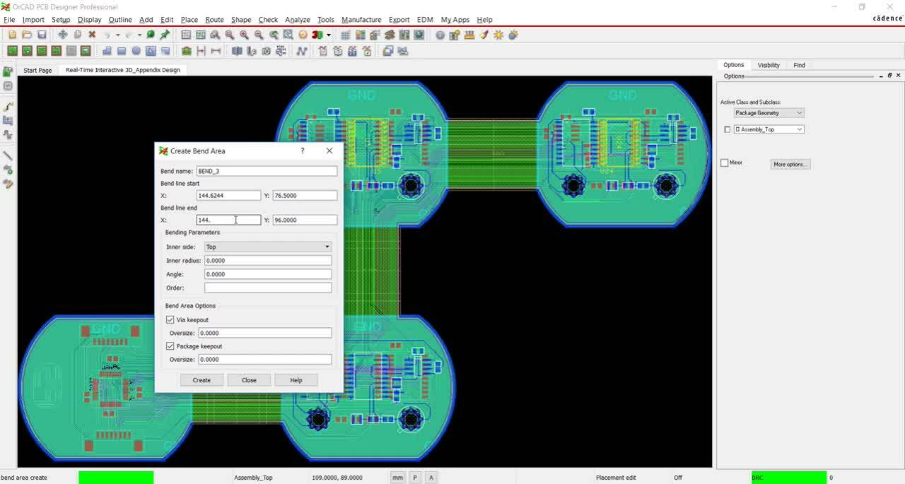
Rigid-Flex Transformation (Bending). This QIR4 release builds upon the recently introduced Bend area capability on the 2D workspace by now allowing designers to transform – also known as bend – flex or rigid-flex designs from a flat 2D state into a transformed 3D state. Designers will now be able to visualize how their designs will look like when they are in their intended state. Designers also have the ability to add STEP models of housings and other such mechanical components to their PCB designs and check for fit and clearance issues.
Thieving with Hexagon Shapes. Thieving is typically added to surface layers to balance the chemical process for PCB plating. PCB Editor supports both surface, internal, and even mask layer thieving patterns. Hexagon shapes now supported in QIR 4 in addition to the legacy circle, rectangle, and line options. Enabling the Packed spacing option updates the spacing X and spacing Y fields providing a consistent spacing around a staggered hexagon pattern as shown in the following image.
Cross Section Chart and Table update. A new field Chart Unit in the Cross Section Chart dialog box permits table units to override database units.
3D Canvas Update (View Video)
3D Canvas Update
New 3D Canvas (Watch Demo Video): Major 3D improvements have been added to OrCAD PCB Editor, delivering higher quality visualization and speed for design planning and viewing in 3D.
Rigid Flex (Watch Demo Video)
Stack up by zone. The new feature improves MCAD-ECAD co-design and provides faster, easier definition of stack-ups for rigid-flex rigid designs.
Inter design layer checks. The new inter layer functionality provides ability to check geometries between two different class/ subclasses for flex and rigid flex designs.
Arc routing. A new prototype feature to provide more efficient method to add routing during Add Connect by following an existing connect line or a route keep-in.
Cross section editor. Redesigned Cross Section Editor based on the spreadsheet technology found in Constraint Manager to provide one stop shop for features requiring cross section for their setup.
New padstack editor. Introducing modern user interface for convenient padstack creation with addition of new geometries and support for counter-bore/ counter-sink definitions and several new drill features. (Watch Demo Video)
Shape Edit Application Mode. Introducing new functionality that is a fine tuning editing environment to increase efficiency with shape boundary editing and simplifying actions such as sliding a shape edge or adding a notch etc.
Color and Visibility enhancements. The Color Dialog box has been enhanced for better efficiency and ease of use for designers and the Visibility pane now provides access and control over layers other than the conductor layers.
64 Bit Support. Now available support for 64 bit OS with increase in memory size from 4GB to 18 Quintillion and support for Database sizes up to 3GB.More gains in performance for CPU intensive applications.
Display segment over voids. A new command Segment Over Voids detects cline segments crossing adjacent plane layer voids. (Watch Demo Video)
Spread Line between Voids. New command to provide semi-automatic solution to spread channel based clines with respect to adjacent plane layer voids.
Via2Via Line Fattening. Users can increase line width between vias based on their definition of edge to edge clearance by using the “Line fattening” utility. (Watch Demo Video)
Contour routing. Now available in both single and multi-routing modes, contour hugging locks the current route to either the route keepin or adjacent cline.
Group routing. User can now perform group routing by window selecting around a group of objects(Clines, Vias, Pins, Rats) and be able to change the control trace from its initial location to user defined and go into single trace mode to complete routes.
Gloss Commands. Richer set of gloss commands like Eliminate Vias, Convert corners to ARC, Fillet and Taper traces and many more now available in OrCAD PCB Designer.
Differential Pair Routing and DRC. Users can now define physical and electrical rules for Differential pairs complemented by routing support.
Layer Set DRC and Routing. The new layer set functionality insures layer constrained nets are routed to wiring requirements by ‘locking routes’ to within the appropriate layer set(s) for the net based objects. (Watch Demo Video)
Large and complex expressions in netlists. You can now create complex expressions of up to 245 characters in netlists. The length of lines in netlist has been increased from 132 to 245 characters.
Enhanced numerical precision. Numerical values can now have a higher precision as the minimum parameter value supported is 1e-80 in comparison to the earlier 1e-33.
Improved convergence. Convergence has been enhanced because of the following new controls for Pseudo Transient Analysis to handle bias point convergence:
PTRANABSTOL: Determines stabilization of currents (capacitor). Default value is 1e-7
PTRANVNTOL: Determines stabilization of voltages (inductor). Default value is 1e-6.
PTRANSTABSTEPS: Sets the maximum iterations to run before stopping. Default is 2100000.
Generating Device Modeling Interface (DMI) independent of Visual Studio versions. The process of Device Modeling Interface (DMI) has been enhanced with the ability to generate Device Modeling Interface (DMI) template independent of MS Visual Studio version. Use use any version of MS Visual Studio to generate DMIs.
PSpice Advance Analysis Enhancements. The new enhancements in PSpice Advanced Analysis (AA) allow users to run PSpice AA on existing designs without the need to update any parts/models of the design. The key functional enhancements including (Watch Demo Videos):
PSpice – MATLAB Interface. The integration of Cadence® PSpice® with MathWorks MATLAB and Simulink provides a complete system-level simulation solution for PCB design and implementation. (Learn More)
Virtual Prototyping. New functionality for automating the code generation for multilevel abstraction models written in C/C++, and SystemC, VerilogA-ADMS, and a set of behavioral analog devices and controlled sources. (Watch Demo Video)
Products Covered: OrCAD Capture | OrCAD PCB Editor | PSpice
Rapid PSpice Model Association. Capture now supports instance-level, PSpice model assignment directly to components in the schematic editor.
PSpice Library Search. Capture now provides an easy method to search through the installed library of simulation models / parts using PSpice Part Search.
Capture View-Only Mode. New view-only mode allows any project / schematic files to be opened for review without consuming a license.
Redefined Quick Place Menu. The Capture Place > PSpice Component menu has been updated with new items and sub-menus including; PSpice Ground, common discrete components, and new sources.
Display Properties Update. New display property option to display a value only if a value exists. Useful for commonly displayed properties like tolerance where you would not want to display the property name if a value does not exist.
Capture View only Mode. Allows Capture to be opened in read-only mode and does not check out a license. Accessible through command line switch capture.exe -viewer.
Zero Pin Mechanical Parts. Mechanical parts with no pins like bar-codes, fiducials and mechanical holes can now be placed on the schematic and synced with the PCB.
SI Flow Updates. The Capture SI flow now supports Sigrity products as well as OrCAD PCB SI.
Object Alignment. Support for horizontal and vertical alignment of objects on a group or signal object level. New alignment toolbar added as well.
Object Distribution. Select and distribute objects evenly or horizontally.
Library Refresh. If libraries are updated outside Capture during an active session users can now perform a library refresh to display the updated information.
Schematic Page Name Property in Titleblock. Titleblock now supports a new system property “Page Name”. The “Page Name” property behaves like the “Schematic Name” property available in previous releases. Any change to the page name automatically synchronizes and updates the value of the property.
SI Flow Update (XNet View). Users can now easily view a filtered list of defined XNets in the current design. View provides data on the XNet included the flatnets that make up the XNets.
New NetGroup Display Options. Can now set NetGroup to display the definition of the NetGroup only if the name of the NetGroup is different from the NetGroup instance.
Common Property Text Justification. You can now justify comment text and the text of displayed properties of any Capture object, such as Parts, Off Page Connectors, and Ports.
Tcl Updates. New Tcl scripting API updates are available for variant customized variables in the titleblock, visibility control on NetGroup alias, and access to project libraries.
Design Date Format Options. Two new options for data format display.
Convert Views. Convert Views supported in PCB Editor netlisting.
Capture – PCB SI Integration and Flow. With product integration comes a new bi-directional schematic entry/signal integrity flow that allows electrical engineers to explore circuit topologies, develop constraints, and analyze signal integrity.
Quick-Place for Common Components. A new menu, Place >PSpice Component, enables quick-place for commonly used schematic or simulation components. The menu items list of components is user-configurable and has been pre-populated with PSpice® simulation devices (passive, discrete, sources, digital).
User-Configurable Menus and Toolbars. Menus, toolbars, and icons in OrCAD Capture, PSpice Advanced Analysis, and Model Editor can now be customized. This makes it possible to run any Tcl method or script from the menus.
Enhancements to the Find Function. The Find function now allows searches for parts by value of a given property (e.g. Property Name=Value) or use of a regular expression as the search string. For example, to search for components with designators starting with C or R and followed by any number between 2 and 9, use the search string Part Reference=(C|R)[2-9].
NetGroup Enhancements. The NetGroup use model is now aligned with the Bus use model for intuitiveness and consistency. Enhancements areas include: assign a NetGroup to a Bus, reorder pins in an unnamed NetGroup, add and remove pins from a NetGroup, visible NetGroup references, and find NetGroup references.
Enhanced Save Function for Design and Library. Pages that are changed and need to be saved are now marked by an asterisk (*) in the Capture Project Manager. When a save is initiated, the marked pages are saved.
Global Replace for OffPage. The Find and Replace dialog box (Edit> Global Replace) has a new option, OffPage Connector, to find and replace OffPage connectors.
Preserve “User-Assigned” Designatos. Reference designator management improvements now track the user-modified references and allow finer end-user control over managing the part references for the entire design. A reference designator can be interactively set as user-assigned through the newly added “User-Assigned” flag to preserve designators and references in conjunction with the Preserve Designator and Preserve User-Assigned Valid References in the Annotate window. Capture will also mark a reference designator as user-assigned if the reference is manually changed in Property Editor, manually changed in the schematic canvas, or changed by the board through back-annotation.
Design Level Auto Reference. In addition to schematic-level annotation, design-level annotation is now available by selecting the Design Level option in the Miscellaneous tab of the Preferences dialog box. An option to preserve references when copying is also available.
Browsing/Viewing Designs Created in Earlier Versions. Designs created using earlier versions of Capture can now be opened and viewed without requiring the design to be uprev’ed. Such designs only need to be uprev’ed when the design is actually saved.
Closing All Tabs. Canvas tabs can now all be closed, or all but this tab closed with an RMB selection. Right-click on the tab and choose the appropriate option (Close, Close All Tabs, or Close All Tabs But This.
Custom Design Rule Check (DRC). Though Tcl scripting, user-defined schematic and circuit checks can be created and added to the Capture DRC routines. Several R&D examples include checks for hanging wires, device pin mismatches, overlapping wires, reference prefix mismatches, port-pin mismatches, and shorted discrete parts.
Project Save As Enhancements. While saving a project in 16.6, a project name that is different from the design name can be specified to mimic the manual process of copying/moving a product from one hard-drive location to another. Options include the ability to copy/move all referenced files, ensuring that all links are updated while saving.
RefDes Support Alignment. Capture and CIS now handle references and designators in the same manner, eliminating the need for manual Reference Designator corrections in the CIS database and BOMs. CIS now supports all reference designator formats including as U2N, C1_R, C12-1, R7-TOP, MP_2V5_REF, and TP3V3_0. Also, the reference designator for multi-packages is consistent (e.g. MP_2V5_REF will be MP_2V5_REF not MP_2V5_REFA).
Linking External Design Parts. Referenced parts of the external design can now be linked at the group or subgroup level.
CIS Performance Increase. The overall performance for CIS operations, especially when dealing with very large databases or queries, has been significantly improved.
Tcl Customization for CIS Explorer. CIS Explorer can be custom-configured with user-definable actions and capabilities. (For example, customized part placement checks can disable placement of an EOL part or provide a warning if part procurement has a long lead time). Query result rows can also be customized. (For example, rows can be highlighted blue for recommended parts or red for parts not recommended or allowed.)
CIS Multi-Value Support. Any CIS field can now be set as multi-valued for component instances with numerous information or content sources (e.g. lists for multiple datasheets/application notes or multiple PSpice models for a component).
PSpice Learning Resources Update. Users can use the new Digital Electronics and Data Convertors chapters with working examples that have been added to the Basic Electronics book in Learning PSpice.
Speed Upgrades. Users can take advantage of the 5 levels of speed upgrades with the default set at a level 3, (speed level should be set at 0 for compatibility with previous releases). The speed levels will allow for faster switching of devices and show substantial improvement from the previous release.
Enhanced Multicore Support. Removed multi-core usage limit (previously maxed out at 4 cores).
Convergence Improvements. With QIR7 improvements, users are recommended to use lower values of ITL4 to achieve convergence and performance compared to previous releases requiring high ITL4 values using Switches circuits to achieve convergence. This will help to eliminate performance and mathematic errors.
Hysteresis Core Loss Calculator. Users can now use this app that measures Steady State loss of energy in a magnetic core for power supplies.
New Simulation Reporting Capabilities. Users are now able to generate an HTML report for Analog Transient simulation where average, RMS, and Peak values of Current, Voltage, and Power can be reported. This is user customizable and there is a TCL source available in the installation hierarchy.
Enhanced PSpice Model Search Utility. Now PSpice Advance Analysis libraries, such as, aa_igbt.olb, and so on are added to the PSpice Part Search database so you are able to search and then place in your designs. The symbol viewer within the Searcher has also been updated.
Object Distribution Feature. Enhanced to force equal spaced distribution by default.
Temperature Sweep for Monte Carlo. With this new PSpice app, multiple runs of Monte Carlo can be run sweeping at different temperatures.
New PSpice Modeling Applications. PSpice modeling applications for Switch, Transient Voltage Suppressors (TVS), Voltage Controlled Oscillator (VCO), Independent Sources, and PieceWise Linear (PWL) Sources have been added to Capture.
Random Function for PSpice Simulation. A new, supported Random function has be added to the PSpice Engine eliminating the previous work-around that required a PieceWise Linear (PWL) source set to auto-repeat.
Frequency Response Analysis. New method to calculate open loop gain for switching circuits from transient analysis using Middlebrook’s Method (blog article).
Learning PSpice Update. Added a new Power Electronics module. Complete theory and design with examples included. Accessible through Help>Learning PSpice.
Comments as OrCAD PSpice Directives. All comments in the Capture canvas starting with @PSpice are net-listed into the .cir file. Used to quickly define commands not available through standard PSpice setup GUI.
Option to Ignore DML Error. New option in the IBIS2Spice command to DML checks and attempt at translating to Spice.
New Convergence Options. The following convergence options are now available in .OPTIONS
Global Parasitics Support Convergence Option. Ability to set minimum parasitics for the following devices
Option to Apply Parasitics Globally. On analysis of a large number of OrCAD PSpice designs, it was found that a number of issues were caused by ideal devices (without parasitics). For example, using an ideal diode with parasitics can lead to convergence and performance issues as the simulator quickly moves to very small timesteps and often goes over minimum timestep thresholds. New options are available to set a minimum parasitics value level for diodes and Bipolar Junction Transistors (BJT) globally.
“10p files for Convergence Failure” Option. This option allows the operating point values even if a convergence failure has occurred, thereby avoiding situations where the user is left with previous bias point values on convergence failure.
CSHUNT On/Off Option. In a number of cases, the nodes values do not stabilize because one or more feedback path has no delay in path. Successive iterations within OrCAD PSpice solver result in node oscillations and convergence errors. The OrCAD PSpice 16.6 QIR 3 provides a CSHUNT option that adds capacitors of specified value to the nodes. While a default value of 1.0E-12 is recommended, it can be changed on a case-by-case basis.
Enable Continuation Methods. This series of transient convergence methods allows OrCAD PSpice simulator to override default solution search schemes and apply other heuristic algorithms, and is applied when all other options have failed. An example of such an algorithm is to reject the last successful time point and start working out the simulation solutions from the time point previous to the last successful time point. Additional heuristic algorithms will be added under this option in subsequent releases.
Learning OrCAD PSpice Technology and Adding Your Own Content. A new chapter is available in the Learning OrCAD PSpice module. This chapter explains the steps required to add your own content, lessons, or app notes to OrCAD PSpice environment.
Subcircuit Definition. Subcircuit definitions in OrCAD PSpice environment can now support any character length.
Fourier Output. Fourier output now supports NUMDGT.
OrCAD PSpice Modeling App. FREE app to enable quick and accurate creation of OrCAD PSpice parts directly on the OrCAD Capture schematic using a wizard-style interface. The first version of the app includes the following model generators. This app can be downloaded at the OrCAD Capture Marketplace
Advanced Control Options. Numerous advanced convergence and simulation control options/parameters have been added or exposed, giving users greater control over simulation and convergence. These options include: bias-point convergence, voltage limiting, worst-case deviations, max-time step control, pseudo transient, and relative tolerance.
Probe .dat Upgrade to 64-bit Precision. OrCAD PSpice technology now generates 64-bit data precision in the .dat file output. This ensures higher precision compared to the 32-bit .dat file data from previous releases. (As an example, in previous releases, when a very small amplitude voltage is superimposed on a large voltage, the resulting voltage lost its resolution in a 32-bit .dat file.).
UNDO Support for Captured Netlists. Netlisting to OrCAD PSpice environment now preserves UNDO, making it easier to make iterations and modify parameters, components, and connectivity.
Enhanced IBIS Support. The IBIS to OrCAD PSpice model now supports V-T curves for all IBIS models up to version 5.0.
Multi-core Engine Support. Enhancements to multi-core support and I/O read-write provide significant performance improvements. Focused performance enhancements, especially for large designs or designs with complex model instances (MOSFETS, BJT), also boost performance.
Encryption Enhancements. Upgraded model encryption now includes 256-bit (AES) encryption support.
Tcl-based Customization. Advanced Analysis, simulation, and .dat file access can be accessed and extended with user-definable actions and capabilities. This enables an environment that can be enhanced to specific flows and needs, and allows users to leverage enhanced features and design capabilities.
Products Covered: OrCAD Capture | OrCAD PCB Editor | PSpice
New OrCAD Suites:
New Models