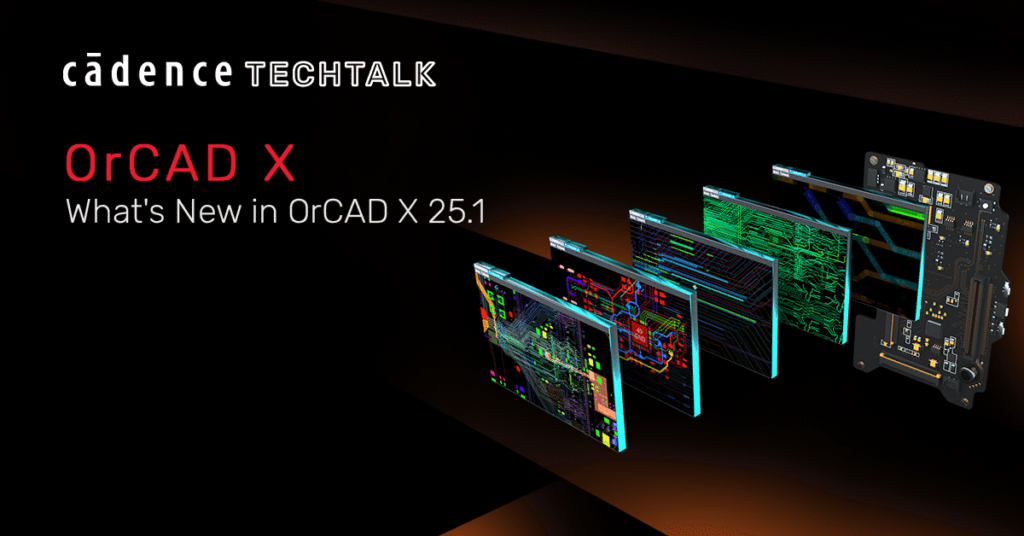
Experience the next generation in PCB Design. More than 40 years in the making OrCAD X is the design platform of choice for teams looking to maximize productivity and value.
OrCAD X is built to accelerate your PCB design process from schematic capture through PCB layout and simulation to seamless error-free manufacture.
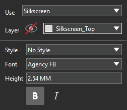
OrCAD X Capture is the industry-standard tool for fast, accurate schematic entry; designed for clarity, reuse, and clean handoff to layout.
Built for fast design entry with:
Always know what changed with seamless sync of data between the schematic and PCB.
Easily define and validate your design intent with real-time design rules checks, constraint definition, and integrated simulation.
Apply constraints and key rules early
Identify issues before layout begins
Shorten review cycles and iterations
Start with access to millions of CAD models from the beginning
Integrated symbols, footprints, and 3D models
Improve consistency across projects
Spend less time building libraries
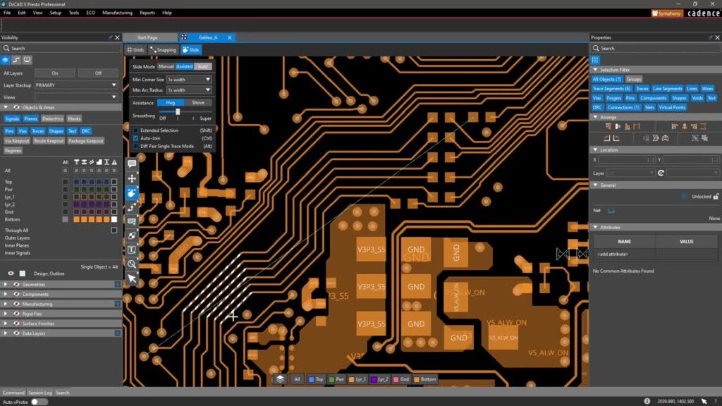
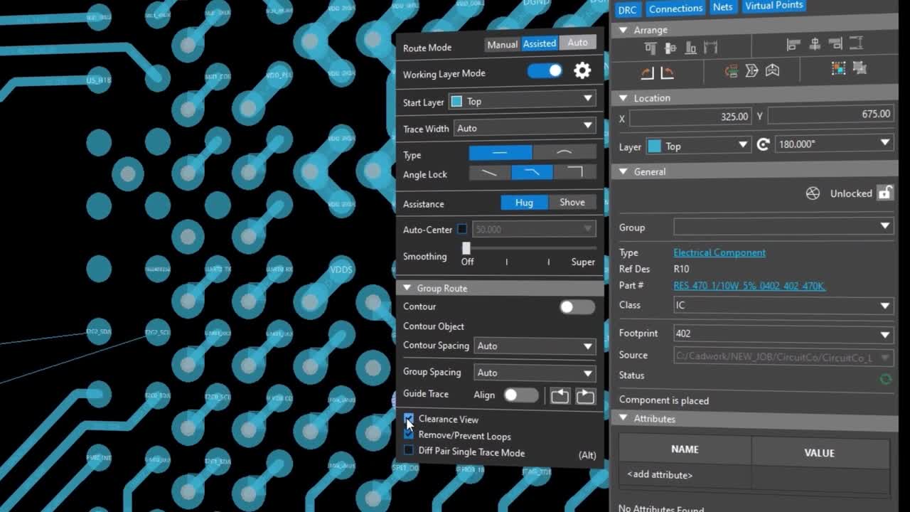
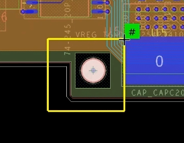
High-performance PCB layout with real-time constraints, automation, and 3D visibility.
Route with real-time guidance:
Don’t wait until the end of the project to find all the issues you need to fix and change. Get instant feedback as you design with on-canvas guidance and notifications, so you can solve issues before they have a chance to become an ECO.
Check fit early and often:
Support modern PCB complexity:
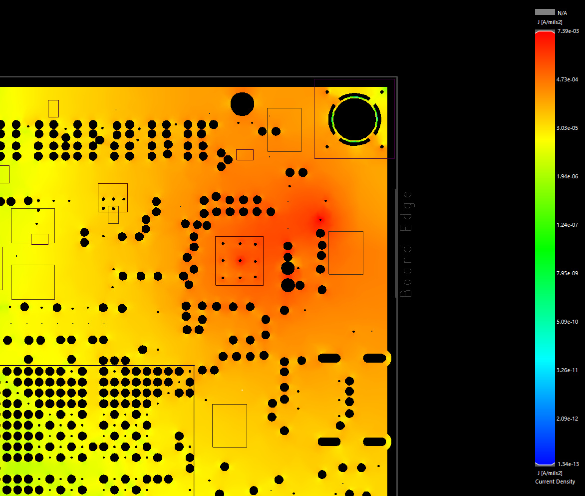
Verify decisions earlier with integrated analysis ensuring issues are found before they become rework.
Ensure design accuracy as you work
Run checks during the design process
Identify electrical risks earlier
Reduce downstream debug and redesign
Make better tradeoffs faster:
Confirm key decisions with analysis
Avoid rework caused by guesswork
Improve confidence before manufacturing
Make simulation a natural part of the design process:
Keep verification tied to the design
Reduce tool switching and context loss
Speed decisions with results in context
Leverage a full suite of analysis engines and explore all aspects of your design from analog mixed-signal, signal integrity, power integrity, and even thermal affects. Mix and match engines easily to meet your design requirements and move to production with confidence.
Prevent manufacturability issues during design to improve first-pass success and reduce respins.
Design for Manufacturing Upfront:
Identify DFM issues earlier in the process
Fix problems before generating outputs
Reduce respins and fab/assy delays
Ensure fit and function by seamlessly synchronizing your design with mechanical before you build.
Generating the correct files and providing accurate and clear documentation is critical for design success. With OrCAD X, ensure a smooth manufacturing process without manual effort by automatically generating your design documentation and manufacturing output files.
Automate and enhance your documentation process with a real-time templated approach to artwork and drawings.
Collaborate across teams with flexible data and library management. Choose cloud-hosted or self-hosted to match governance needs.
Effortlessly manage your libraries with access to OrCAD CIS library management either on premise or in the Cadence cloud. Enable your teams to seamlessly share, manage, and leverage a single source of truth for your part libraries. Get rid of the needless email chains and finger pointing to try and figure out who changed what when. Easily manage files, design revisions, and complete design version history at your fingertips.
Design together effectively
Share design context for faster decisions
Support review and markup workflows
Reduce miscommunication across teams
Ensure your products will breeze through manufacturing and be able to stand the test of time with built-in supply chain insights.
Your design is often part of a whole and as such, will need to be managed in a company PLM system or similar. Easily synchronize your design data with PLM and surface contextual data from PLM such as corporate-approved part numbers directly in your CAD tool and ensure a smooth transition to production.
See how teams reduce respins, speed layout, and hit deadlines with OrCAD X.
Solve your tough design challenges with the advanced features and flows in OrCAD X
OrCAD X is consistently being improved with major new features added every year.

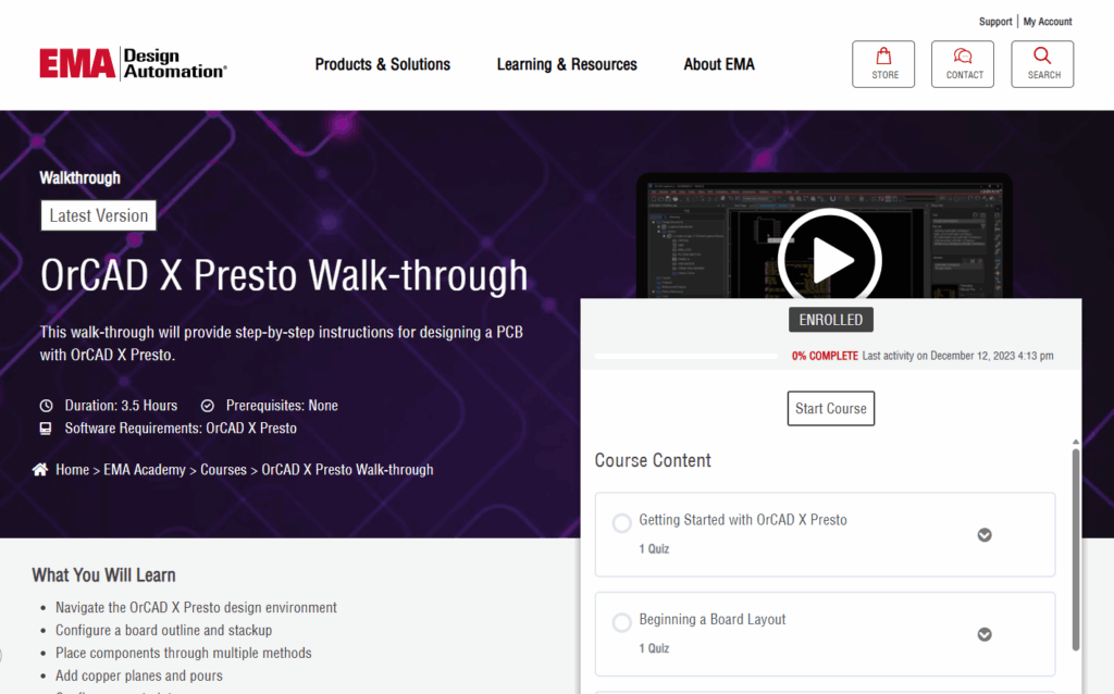
Get instant access to our library of training and how-to materials to help you get up to speed quickly.
Choose the OrCAD X PCB Suite that best fits your design needs today with the ability to seamlessly scale tomorrow for increased capability when you require it.
Need help choosing? Contact us and we would be happy to answer any questions.
Get the latest insights and information
Over 30 years’ experience helping engineers design, validate, and build hardware successfully.
OrCAD X is the next generation of OrCAD and as such is built on and contains all that is OrCAD today and expands on it with entirely new user experiences and functionality geared to help designers tackle the next generation of design challenges with confidence. OrCAD X gives you access to all the tools you have with OrCAD now so that you can leverage what works best for you and make decisions on which capability and UX to use when for yourself. The goal is to provide you with truly game changing technology, but we do not want to assume on your ability or timelines for adopting these new tools.
You can visit our release history to get more details about the capabilities being added in this release. OrCAD X is on an annual major release cadence with patch releases pushed out throughout the year.
OrCAD users who are active on maintenance are able to seamlessly upgrade to OrCAD X! Please contact us and we will contact you to get the process started.
Yes! Unlike other vendors that require you to all have the same tier software regardless of your individual license and functionality needs OrCAD X allows you full freedom to select the combination of products and licenses you need all while maintaining full file and library compatibility for maximum collaboration and reuse. This also extends to Allegro X allowing for a wholistic design environment across your entire organization.
Yes! OrCAD X comes with importers for popular CAD formats making it easy to transition your designs and libraries should you choose to. We also offer migration services if you are looking for a white glove approach to your transition.
No. Cloud use is not required and is entirely optional. If you workflows or security requirements do not allow usage of an external cloud environment you can leverage OrCAD X without any cloud connection at all. If you are able and do want to leverage the cloud to help speed up workflows and collaboration you can learn more about the cloud solutions here.
Yes! Since OrCAD is fully compatible and scalable to Allegro and OrCAD X is fully compatible with OrCAD, you can seamlessly share designs and data with counterparts using the Allegro / Allegro X platform.
Yes! You can request a free 30 day trial or contact us and we’d be happy to get you setup.
OrCAD X Supports Windows 10 and Windows 11. For full hardware specs you can view the current hardware requirements (link). If you are looking for Linux support, Allegro X offers both Windows and Linux support.
Yes. We offer multiple license types to help best match your needs. License options for OrCAD X can broken down in the following categories:
License Term | Access | Description |
Perpetual | Floating | Shared license that can be accessed by any user (1 user per license concurrently). License is valid for 99 years with the option to purchase support annually for technical support and product updates. |
Time-Based | Floating | Shared license that can be accessed by any user (1 user per license concurrently). License is valid for a specified period (usually 1-3 years) with support and product updates included during the term the license is active. |
Time-Based | Single-User | Named user license that can be installed and accessed on up to 5 computers. License is authorized for use by specific user. |
*Additional options are available for users wanting to share license access across regions (WAN).
While OrCAD X is designed to be intuitive and easy to use from the start, we offer a full set of training courses to help users get to up to speed quickly and effectively. From on-site instructor-led courses to free on-demand training we have what you need to make sure you are getting the most out of your software investment. Visit the EMA Academy to learn more about training and learning resources.
Yes, we do! Students are eligible to receive free access to OrCAD to use as part of their studies. We also offer free training, sample curriculum, and license for use in labs and classroom settings. You can learn more about our university and educational programs here.
Yes. We do have programs and offers to help startups and new business get access to the design tools they can grow with. Contact us for more details to see if you qualify.
Yes. You can always download and run older versions as needed as part of your license. Files are cross version compatible allowing to work with users on different revisions if needed as well.
Yes. We offer an extensive list of integrations to other tools, PLMs, and systems. You can also build your own with the extensive scripting environment available. Let us know if you have specific connections, you are looking for or would be interested in our team helping with custom integration services.