Advanced Package Designer (APD)
Effeciently, design, verify, and optmize complex packages with first-pass success
The Market Leader for Advanced Package Design
Cadence has been leading the way in package design since the start. With a dedicated focused effort on building solutions to meet current and future packaging technology needs. You can be confident that you can enable your package design efforts to become a key value center within your organization.

Cross Platform IC Package Board Co-Design
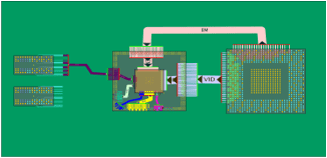
Cadence provides the only platform built to allow you to design and optimize the entire system from chip, package, and board for true multi-fabric design. With direct connections to Virtuoso (link is external) and Innovus (link is external) for chip implementation and tight integration with Allegro for package and PCB analysis design teams are finally able to design with the entire system in mind. Drive next generation design closure faster and more reliably than ever before.

Designed Specifically for Advanced IC Packaging
Many IC package designers have been stuck using tools and processes roughly shoehorned to try and meet their needs. With the complexity and value that can be derived from modern packaging technologies these methodologies are simply not feasible anymore. Cadence Advanced Packaging technology has been built from the start with package designers in mind. With countless successful tape-outs from all processes you can feel confident that as your design complexity increases and your schedules shrink Cadence APD+ is here to help you succeed.

Next Generation Analysis & Verification
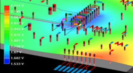
No one wants design failures especially when they could have been prevented if the designer just had the proper information available upfront. Cadence enables design teams to fully characterize their designs before they are built with advanced 3D EM extraction (link is external) technology that unlocks new levels of performance, capacity, and accuracy. With these hyper accurate models you can leverage industry leading Sigrity technology to do complete signal integrity, power integrity, and thermal (link is external) analysis at all aspects of the design from chip, package, and board. Let others guess and hope. Know your design is ready and optimized to perfection with Cadence.
Any Technology. Any Process.
Cadence APD+ leads the industry with the most comprehensive support for the latest packaging techologies. Design with confidence knowing APD has been proven on countless designs even at the most advanced nodes.
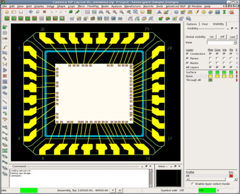
Lead Frame
Mechanical interfaces and advanced wirebonding
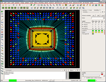
Wirebond PBGA
2D & 3D DRC checking. All-angle/radial routing
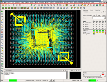
Flip Chip BGA
High capacity HDI structures & routing
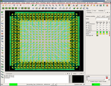
ChipScale Package (CSP)
Die stacking, HDI structures & routing
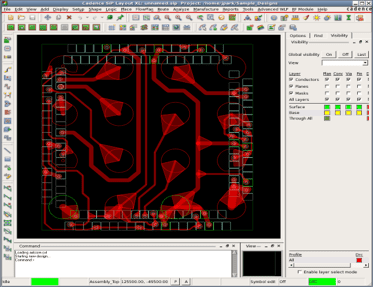
Fan-in WLP (WLCSP)
Merged IC & package layout with GDSII output
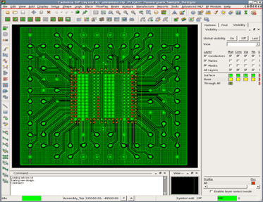
Fan-Out WLP (FOWLP)
Advanced outgassing with GDSII output
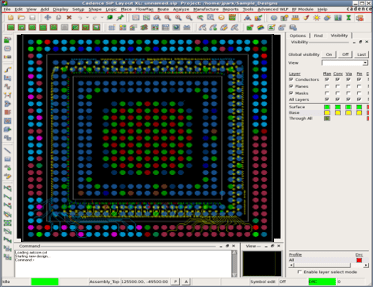
Package on Package (PoP)
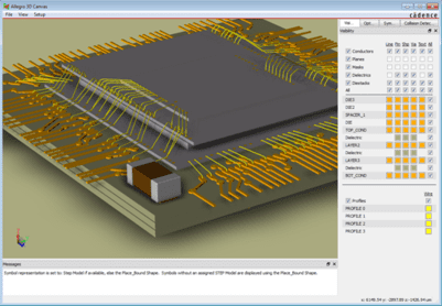
3D visualization & DRC, Auto signal assignment
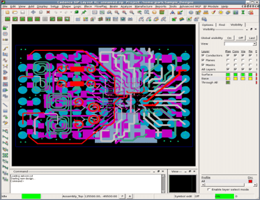
RF Module
Virtuoso integration, Parametrized structures
When You Need More Than Moore
The laws of physics are just one barrier straining the viability and effectiveness of Moores law. New system in package (SiP) technologies such as silicon interposers, 3D-IC, stacked die, etc are enabling companies to achieve the performance, cost, and schedule requirements they need without trying to re-write the physics textbook.

What Our Customers & Partners Are Saying

Request a Demo
See what the advanced packaging technologies from Cadence can do for you.
Schedule a session with one of our packaging experts.