The PCB layout process is like a puzzle with numerous possible solutions. With many components in the design, achieving a layout that is optimized for routing can be difficult and time-consuming. This is especially true when using manual methods to group components including cross-referencing the schematic for connectivity and placing each individual component. With the PCB Clustering App in OrCAD PCB Designer, you can:
- Automatically group components based on schematic page
- Create functional circuit blocks
- Quickly layout a design
This how-to will provide step-by-step instructions on how to use the PCB Clustering App in OrCAD PCB Designer to efficiently group components and layout the PCB design.
To follow along with this tutorial, use the provided design above the table of contents.
How-To Video
Configuring PCB Clustering
Step 1: Open the provided design in OrCAD PCB Designer.
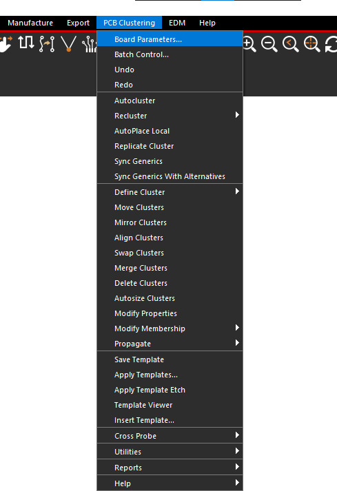
Step 2: Select PCB Clustering > Board Parameters from the menu.
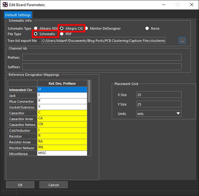
Step 3: The Edit Board Parameters Window will appear. For the Schematic Type, select Allegro CIS.
Step 4: Select Schematic as the File Type.
Step 5: Browse for the Tree-list export file and select clustering_treelist.txt included in the provided files. Select Open.
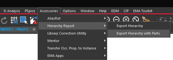
Note: The Tree-list file can be exported within OrCAD Capture by selecting Accessories > Hierarchy Report > Export Hierarchy with Parts.
Step 6: Select OK.
Automatic Component Clustering
Step 7: Select PCB Clustering > Autocluster from the menu.
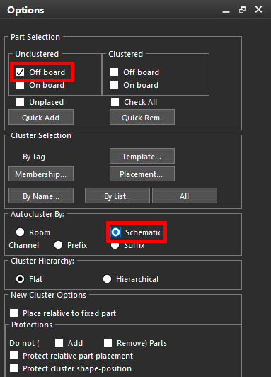
Step 8: In the Options tab, under Part Selection, check Unclustered > Off Board.
Step 9: Under Autocluster by, select Schematic.
Step 10: Select Quick Add.
Note: The components placed off the board which are not clustered have been selected for clustering.
Step 11: Right-click on the schematic canvas and select Done.
Note: The PCB Clustering App will automatically cluster the design.
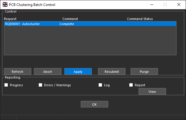
Step 12: The PCB Clustering Batch Control window is activated. Select Apply and OK.
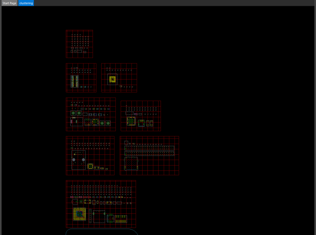
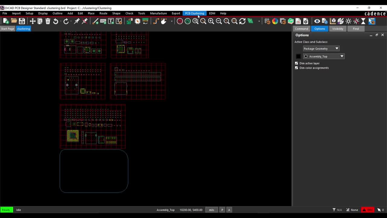
Step 13: View the clustering. The PCB Clustering App has grouped the circuitry based on the schematic pages and circuit functionality.
Note: These groups can then be moved onto the PCB and components can be quickly arranged based on schematic connectivity.
Moving the Grouped Components
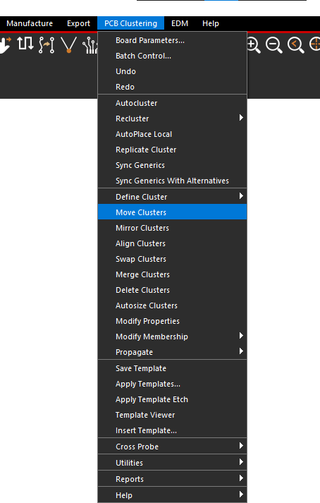
Step 14: Select PCB Clustering > Move Clusters from the menu.
Step 15: Select the cluster to attach it to the cursor.
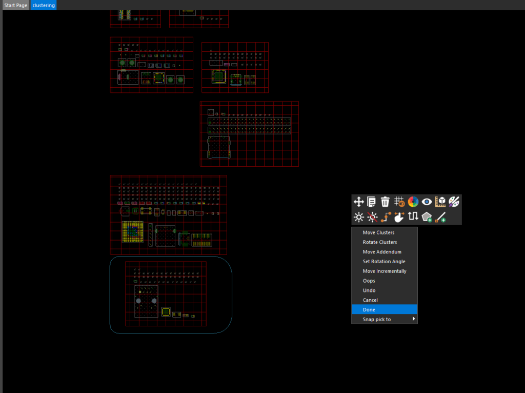
Step 16: Click to place the cluster within the board outline. Right-click and select Done.
Wrap up & Next Steps
Quickly group components based on functionality and efficiently layout the PCB with automatic clustering in the PCB Clustering App. This app and others are part of the EMA Toolkit, one of the benefits of EMA Support +. The EMA Support + program is available to all EMA customers on active support and includes additional benefits and tools to expedite the PCB design process, such as time saving apps, additional training, and more. See what’s included with EMA Support + and learn how to get access to these exclusive benefits.
