Probes and Simulation
This walk-through demonstrates how to setup a PSpice simulation. After you complete this topic, you will be able to:
- Perform bias point and DC sweep simulations
- Add traces to a plot
- Add voltage probes to the circuit
- Export simulation information
To follow along, continue working with the design completed in PSpice Walk-through 3 or open the provided board file in the folder directory, PSpice Walk-through 4_Probes and Simulations.
If Materials were not downloaded in the beginning of the walk-through, they can be accessed through the Materials tab above for this lesson.
 Open in New Window
Step 1: Double click on 0VDC of V1.
Step 2: Change the value to 5V and click OK.
Step 3: Select PSpice > New Simulation Profile from the menu.
Step 4: Name the Simulation Profile Bias_Point and click Create.
Note: The Inherit From drop list provides the ability to create a new simulation from scratch or copy a simulation profile from another project. Setting Inherit From as None will create a new simulation with default settings.
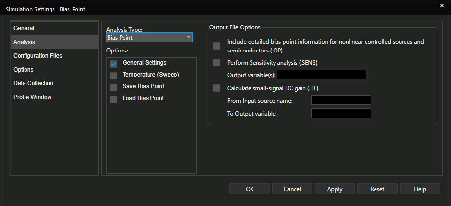
Step 5: In the Analysis Type drop-down, select Bias Point and click OK.
Note: Bias Point Simulation show values of voltage, current and power in your circuit at a bias point.
Step 6: Select PSpice > Run from the menu.
Note: This will invoke the PSpice A/D Window. A bias point simulation will not show anything in this window.
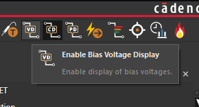
Step 7: Back in the schematic, use the Enable Bias Display buttons on the toolbar or select PSpice > Bias Points to view the values for Voltage, Current, and Power.
Step 8: Select PSpice > New Simulation Profile from the menu.
Step 9: Name the Simulation Profile DC_Sweep and click Create.
Step 10: In the Analysis Type drop-down, select DC Sweep.
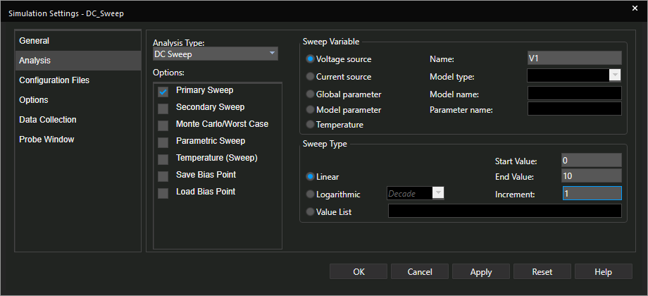
Step 11: Set the Sweep Variable as Voltage Source and assign V1 for the name.
Step 12: Set the Sweep Type to Linear.
Step 13: Set the Start Value to 0.
Step 14: Set the End Value to 10.
Step 15: Set the Increment to 1.
Step 16: Click OK.
Step 17: Select PSpice > Run from the menu.
Note: The PSpice A/D window is blank as no probes were placed in the schematic.
Step 18: In the PSpice A/D window, select Trace > Add Trace from the menu (Insert).
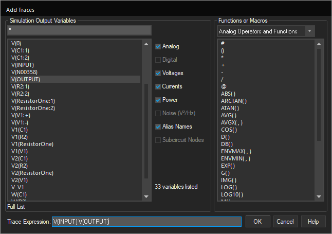
Step 19: In Simulation Output Variables, select V(input) and V(output).Click OK.
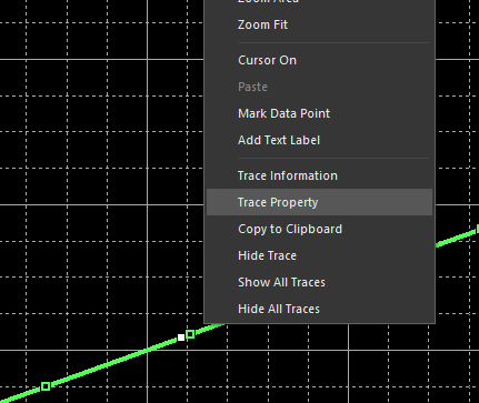
Step 20: Right click on the V(Input) trace and select Trace Property.
Note: Here you can select the color, width, and pattern for the trace.
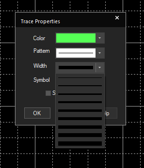
Step 21: Change the Width and click OK.
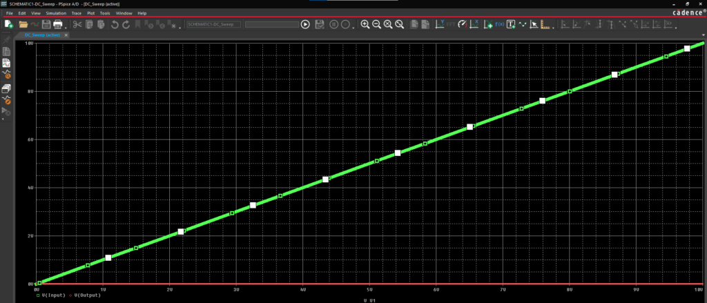
Step 22: View the PSpice A/D window and Close.
Step 23: In the schematic, select the Voltage Probe button on the toolbar or select PSpice > Markers > Voltage Level from the menu.
Note: Voltage probes can be placed on any node.
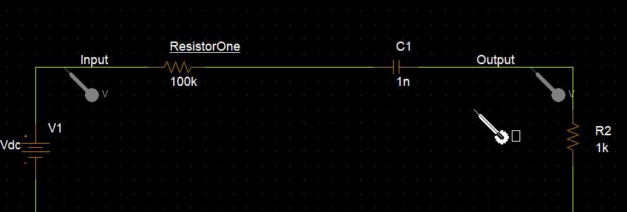
Step 24: Click to place a probe at the Input and Output.
Step 25: Right-click and select End Mode (ESC).
Step 26: Select PSpice > Run from the menu.
Step 27: View the PSpice A/D Window.
Step 28: Back in the schematic, select the probes and press Delete.
Note: If you need to copy the plot, select Window > Copy to Clipboard from the menu. Select the desired view settings. Paste (CTRL+V) the plot into a document. If you need the data points, select the desired trace and Copy (CTRL+C). Paste (CTRL+V) the data points into a spreadsheet. To export a CSV file, select File > Export > Comma Separated File.