Capture Walk-through 12: Netlisting
This walk-through demonstrates how to generate a netlist and new layout file for your Capture 17.4 schematic. After you complete this topic, you will be able to:
- Create a new PCB layout and netlist for the design
To follow along with this tutorial, continue with your design from Capture Walk-through 11 or use the included design file, CAPTURE TUTORIAL 12_NETLISING.DSN under the ‘materials’ tab.
 Open in New Window
- Select PCB > New Layout from the menu.
Note: This will activate the New Layout window where you can create a new PCB layout and netlist your design in one step.
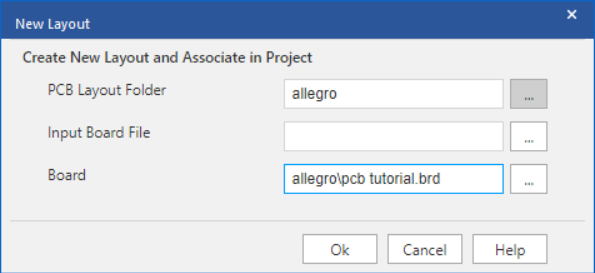
- Browse for PCB Layout Folder to the location the PCB design files should be saved.
Note: Leave Input Board File blank as we are creating a new design. Under Board you can rename the design file if necessary.
- Select OK.
Note: The layout file and netlist output files have been added to the project hierarchy.
- Select OrCAD PCB Designer Professional from the software selection window.
Note: This will open the new PCB layout file, which will be used in the PCB Walk-through video series.
To create only a netlist:
- Select Tools > Create Netlist from the menu.
- With the PCB tab selected, check Create PCB Editor Netlist.
- Browse to the location to save.
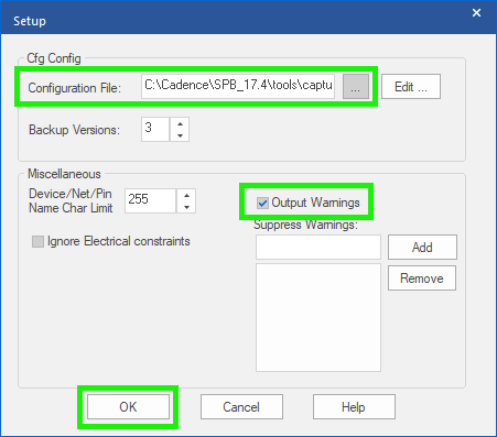
- If this is your first time netlisting, select Setup.
- Browse to the location of the allegro.cfg file.
- Click OK to close the setup.
- Click OK to netlist the design.