Getting Started
This topic will assist in setting up the downloaded design files, allowing you to follow along with the OrCAD PCB 22.1 Walk-through series.
 Open in New Window
Downloading Materials
Step 1: Select the Materials tab for this lesson.
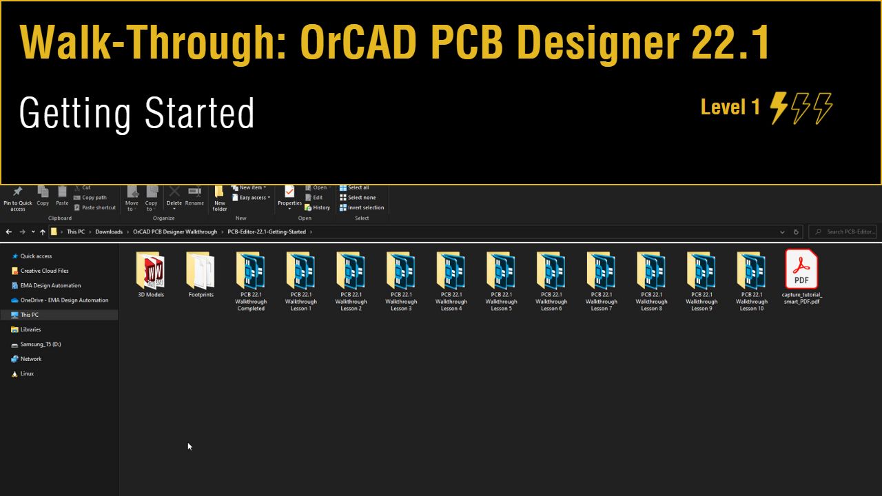
Step 2: Click to download the PCB Editor 22.1 Getting Started.zip file to your computer.
Step 3: Extract the file to your working directory.
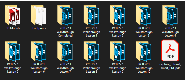
Note: This directory contains a folder containing the completed design, a Smart PDF of the referenced schematic, a folder containing PCB footprints and padstacks, and a folder containing 3D STEP models. Each lesson provides a folder containing starting design files for that lesson.
Configuring Files
Note: If you followed along with the OrCAD Capture 22.1 Walk-Through, the remaining steps can be skipped as they were already completed.
Step 4: From the provided materials, open the Footprints folder.
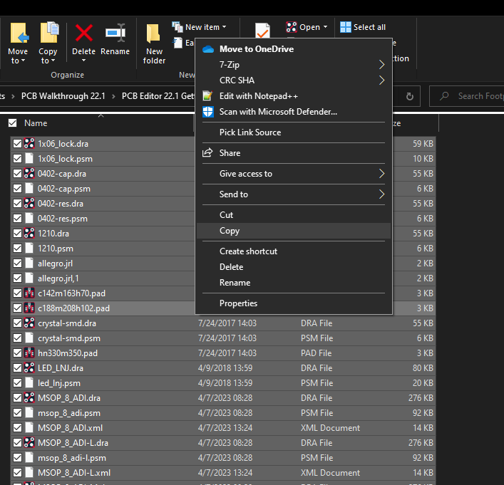
Step 5: Press CTRL-A on the keyboard to select all files and press CTRL-C to copy.
Step 6: In another window of File Explorer, navigate to the standard OrCAD PCB Footprint and Padstack library location: C:\Cadence\SPB_22.1\share\pcb\pcb_lib\symbols.
Step 7: Paste the files to this location.