Lesson 1: PCB Setup
This walk-through demonstrates how to setup the board configuration in OrCAD PCB Designer 22.1 (2022). After you complete this topic, you will be able to:
- Setup and edit design parameters
- Add a layer to the board stack up
To follow along, open the provided PCB_TUTORIAL.brd file in the provided materials or continue with the generated .brd file from the Capture walk-through.
Note: If materials were not downloaded at the start of the walk-through, they can be accessed in the Materials tab of this lesson.
 Open in New Window
Configuring Design Parameters
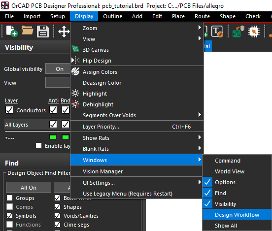
Step 1: Select Display > Windows > Design Workflow from the menu to enable the Design Workflow.
Note: The Design Workflow acts as a design guide, listing all options required for a design in the same place. More experienced users can access design options directly from the menu.
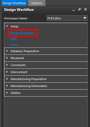
Step 2: Select the arrow to expand the Setup options in the Design Workflow. Select Design Parameters.
Note: In the Design Parameter window, you can specify parameters for display, design, text, shapes, routing, and manufacturing.
Step 3: Select the Design tab.
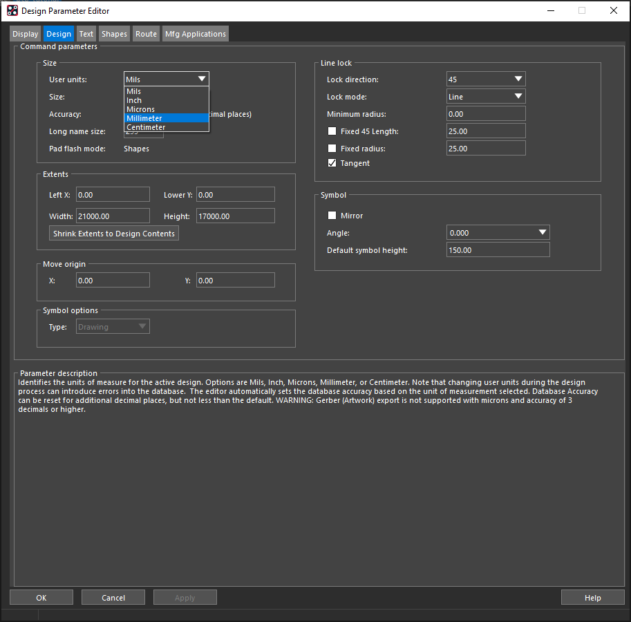
Step 4: Select Millimeter from the User Units drop-down menu.
Step 5: A prompt will appear saying that changing the unit could cause issues with design accuracy. The design has not been drawn yet, so this warning can be ignored. Click OK.
Step 6: Click OK in the Design Parameter Editor.
Step 7: Select Setup > Grids from the Design Workflow.
Note: This can be accessed in the menu by selecting Setup > Grids.
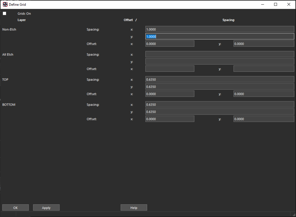
Step 8: For Non-Etch, enter 1 in the X and Y input fields for Spacing.
Step 9: Click OK.
Step 10: Select Setup > Colors from the Design Workflow.
Note: This can be accessed from the menu by selecting Setup > Colors or the Color192 icon from the toolbar.
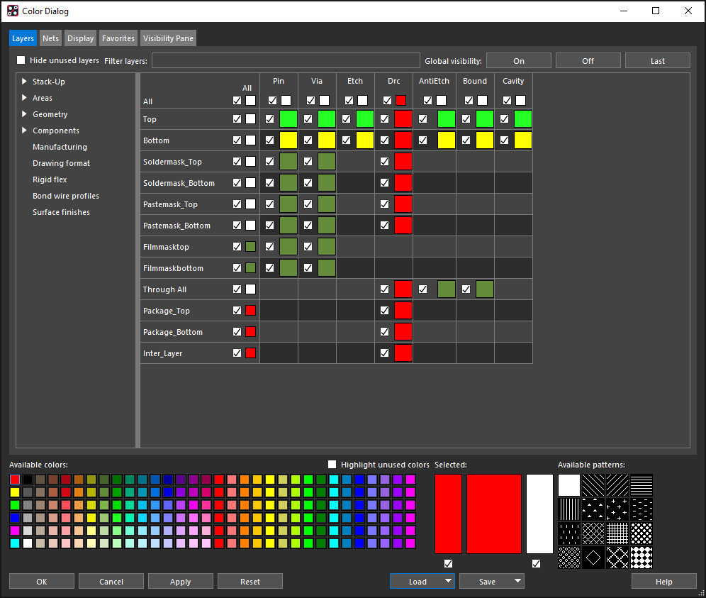
Step 11: View the Color Dialog window. Here you can specify design colors for layers, nets, and more.
Step 12: Leave the default settings and close the window.
Creating the Board Outline
Step 13: Expand Database Preparation in the Design Workflow.
Step 14: Expand Board Outline and Create.
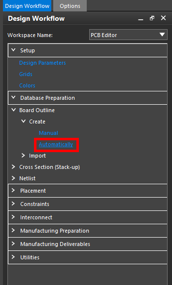
Step 15: Select Database Preparation > Board Outline > Create > Automatically.
Step 16: The Design Outline window opens. Select Create under Command Operations.
Step 17: Set the Design Edge Clearance to 0.3mm.
Step 18: Select the option for Place Rectangle.
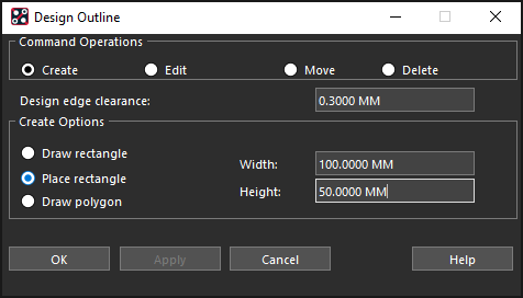
Step 19: Enter 100mm for the width and 50mm for the height.
Step 20: Click to place the rectangle in the middle of the design canvas. Click OK to close the Design Outline window.
Note: Placing the board in the middle of the canvas will leave enough room for the required drawing items later in this walk-through. Use the mouse wheel to zoom out to view the entire design canvas. Do not ‘x’ out of the Design Outline window or click cancel. The Board outline will not be placed.
Creating the Stackup
Step 21: In the Design Workflow, expand Cross Section (Stack-up).
Step 22: Select Cross Section (Stack-up) > Create.
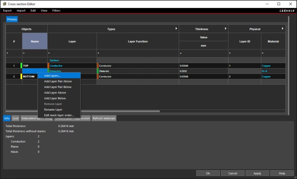
Step 23: The Cross-Section Editor window opens. Right-click in the Name column for the dielectric and select Add Layers.
Step 24: Enter POWERPLANE for the Name Prefix.
Step 25: Select Below Selected Dielectric for the New Layer Position.
Step 26: Select Plane from the Layer Type list.
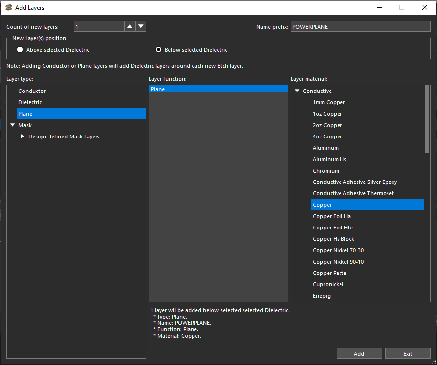
Note: The Layer material can be configured by selecting the desired layer type and function. A default material is selected automatically.
Step 27: Click Add, then Exit.
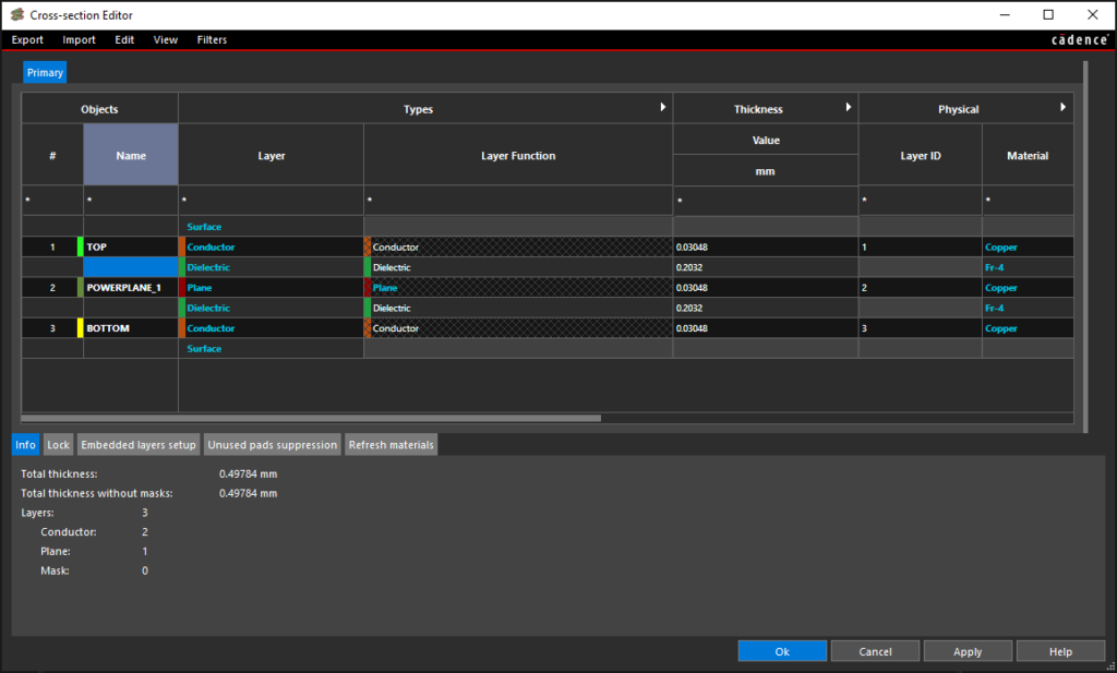
Step 28: The new POWERPLANE_1 layer has been created. Click OK to save the changes and close the Cross-Section Editor.
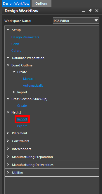
Note: This walk-through has automatically imported the netlist with the PCB creation. If you need to import a netlist, select Netlist > Import in the Design Workflow or Import > Netlist from the menu. Select Design Entry CIS and set the import directory as the folder location of your netlist. Click Import.
Changing the Origin
Step 29: Select Setup > Change Origin from the menu.
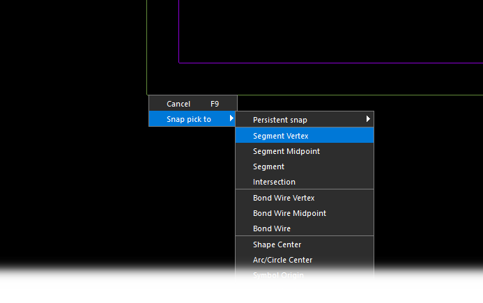
Step 30: Right-click the lower-left corner of the outline and select Snap Pick To > Segment Vertex.
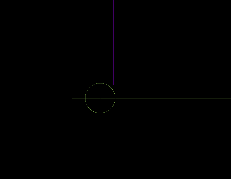
Note: An origin symbol will appear confirming the change.