Lesson 10: RF Amplifier
This walk-through will show how to create an RF amplifier. After you complete this topic, you will be able to:
- Place generic PSpice components
- Place components from the included PSpice libraries
- Create component models with the Modeling Application
To follow along, continue with the design from the previous topic or use the provided materials.
If materials were not downloaded at the beginning of the walk-through, files for this lesson can be accessed through the materials tab above.
 Open in New Window
Modifying the Circuit
Step 1: Click and drag a box around the contents of the circuit to select everything. Hold CTRL on the keyboard and click V1 and Q1 to deselect the components.
Step 2: Press Delete on the keyboard.

Step 3: Click and drag Q1 to move it further to the right. Click and drag V1 to move it further to the left and down.
Step 4: Double-click the value of V1.
Step 5: Enter a value of 15V and click OK.
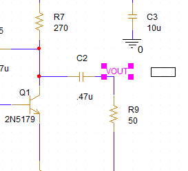
Placing Resistors
Step 6: Select Place > PSpice Part > Resistor from the menu.
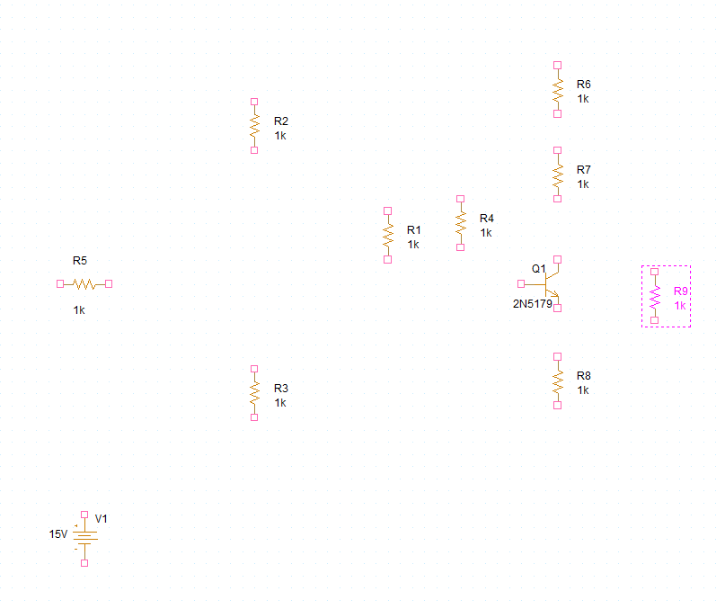
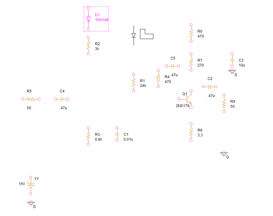
Step 7: Click to place the resistors in the schematic as shown above. When finished, right-click and select End Mode.
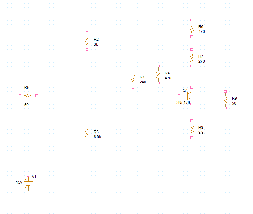
Step 8: Change the values for each resistor to the numbers shown above.
Note: To change this, double-click the value. Enter the desired value and click OK.
Placing Capacitors
Step 9: Select Place > PSpice Part > Capacitor from the menu.
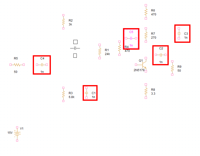
Step 10: Click to place the capacitors in the schematic as shown above. When finished, right-click and select End Mode.
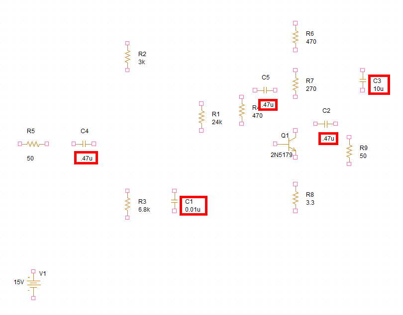
Step 11: Change the values for each capacitor to the numbers shown above.
Note: To change this, double-click the value. Enter the desired value and click OK.
Placing Grounds
Step 12: Select Place > PSpice Part > PSpice Ground from the menu.
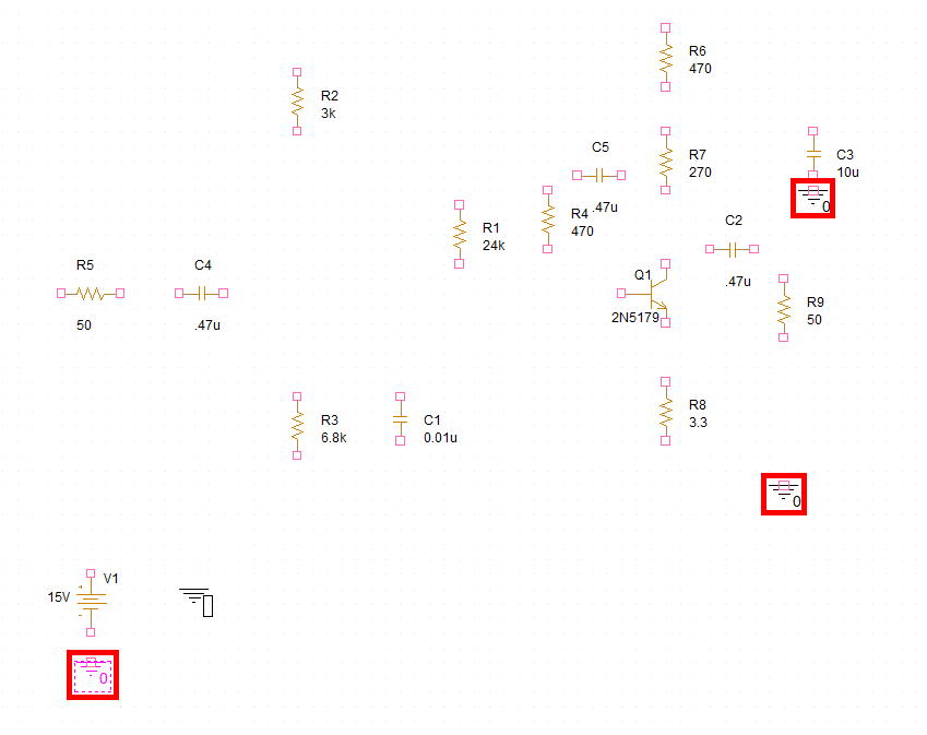
Step 13: Click to place the grounds. When finished, right-click and select End Mode.
Placing Discrete Parts
Note: Generic discrete parts can be placed from Place > PSpice Part > Discrete.
Step 14: Select Place > Component from the menu.
Step 15: Select PSpice from the Categories.
Step 16: Enter 1N4148 into the Search Here field at the top of the table. Click the Search icon.
Note: This will return all components containing “1N4148” in the name or description.
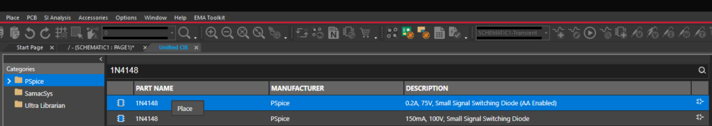
Step 17: Select the first instance of the 1N4148, right-click and select Place.
Step 18: Click to place the diode on the schematic. Right-click and select End Mode.
Step 19: Back in the Unified CIS tab, enter 2N3905 into the Search Here field.
Step 20: Select the first occurrence of the symbol, right-click, and select Place.
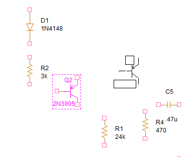
Step 21: Click to place the transistor in the schematic. Right-click and select End Mode when finished.
Placing a Sine Source
Step 22: Select Place > PSpice Part > Modeling Application from the menu.
Step 23: Expand Sources and select Independent Sources.
Step 24: Select the Sine tab.
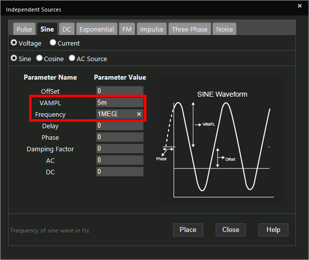
Step 25: Enter 5m for the amplitude and 1MEG for the frequency. Click Place.
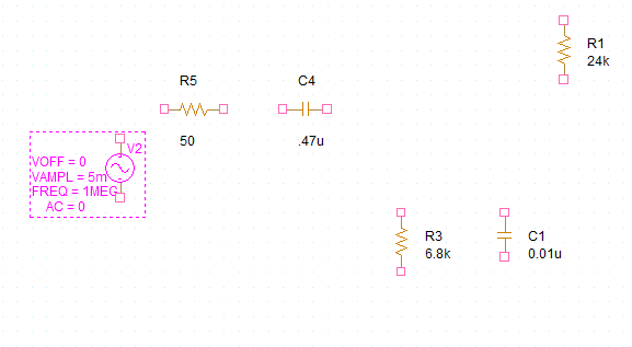
Step 26: Click to place the source in the schematic.
Step 27: Select a ground symbol in the schematic and copy it with CTRL-C on the keyboard.
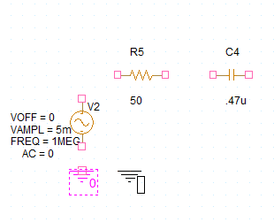
Step 28: Use CTRL-V to paste and click to place a ground symbol at the negative terminal of the source.
Wiring the RF Amplifier
Step 29: Select Place > Wire from the menu, the Wire button from the toolbar, or press W on the keyboard.
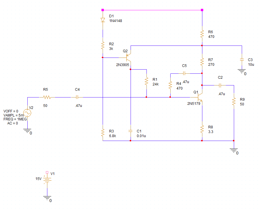
Step 30: Click to begin drawing a wire and click again to finish. Wire the schematic as shown above.
Step 31: Draw short wires at the terminals of V1 and at the top of the circuit.
Adding Net Aliases
Step 32: Select Place > Net Alias from the menu, the Net Alias button from the toolbar, or press N on the keyboard.
Step 33: Enter VCC for the alias and click OK.
Step 34: Click to place the alias on the short wires at the positive terminal of V1 and the circuit.
Note: This will connect the nets electrically.
Step 35: Right-click and select Edit Properties or press N on the keyboard.
Step 36: Change the alias to VIN and click OK.
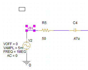
Step 37: Click to place the alias at the positive terminal of sine source V2.
Step 38: Right-click and select Edit Properties or press N on the keyboard.
Step 39: Change the alias to VOUT and click OK.
Step 40: Click to place the alias at the output of the circuit. When finished, right-click and select End Mode.
Note: The VIN and VOUT net aliases will make it easier to keep track of simulation traces.
Configuring the Simulation
Step 41: Select PSpice > Edit Simulation Profile from the menu.
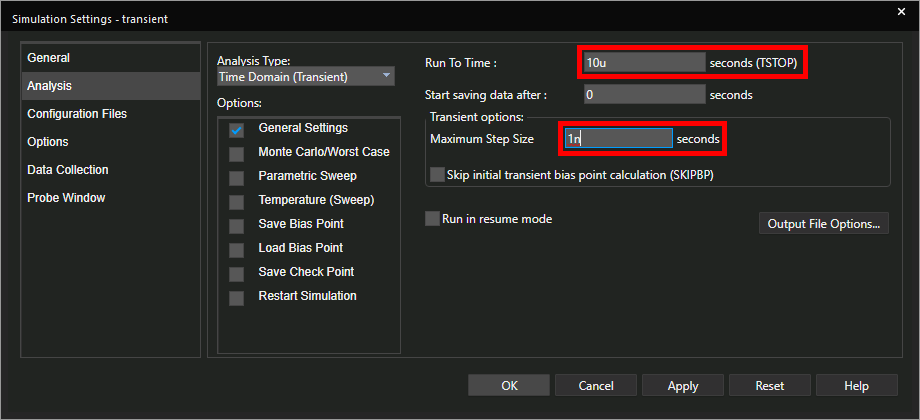
Step 42: Change the Run To Time to 10u and the Maximum Step Size to 1n. Click OK.
Step 43: Select the Voltage/Level Marker button from the toolbar.
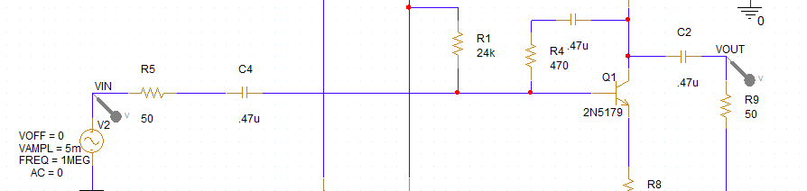
Step 44: Click to place probes at VIN and VOUT to measure the amplifier input and output. When finished, right-click and select End Mode.
Step 45: Select PSpice > Run from the menu to run.
Note: This will run the transient simulation defined in a previous walk-through.
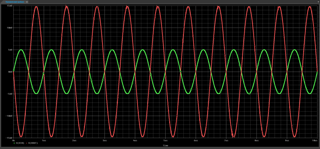
Step 46: View the simulation results.
Note: The output sine wave is amplified, as expected.