Lesson 12: Netlisting
This walk-through demonstrates how to generate a netlist and new layout file for your Capture 22.1 (2022) schematic. After you complete this topic, you will be able to:
- Create only a netlist
- Create a new PCB layout and netlist in one step
To follow along, continue with the design from the last topic or use the provided design files. If the design files were not downloaded in the beginning of the Capture Walk-Through, the design files for this lesson can be found under the Materials tab.
 Open in New Window
Creating a Netlist
Note: This creates only a netlist. To create both a PCB Layout and netlist in one step, move ahead to Creating the PCB Layout.
Step 1: Select the capture_tutorial.dsn file in the Project Manager.
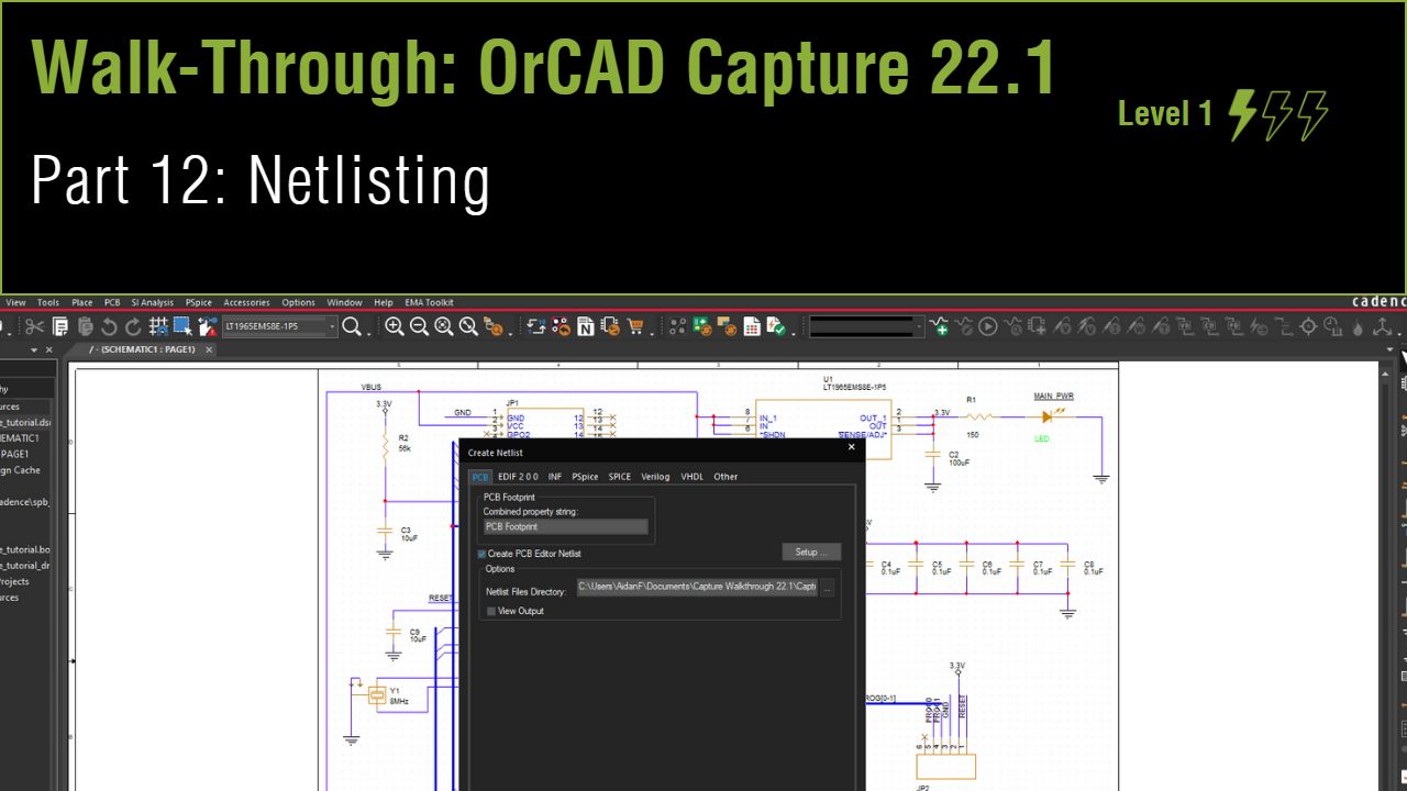
Step 2: Select Tools > Create Netlist from the menu. The Create Netlist window opens.
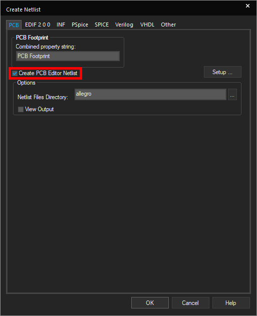
Step 3: Under the PCB tab, check Create PCB Editor Netlist.
Step 4: Under Options, select the ellipsis to browse for a location to save the netlist.
Step 5: The file browser opens. Select the desired folder to save the netlist in and click Select Folder.
Note: Typically, this is a subfolder within the project folder named allegro.
Step 6: If this is your first time netlisting, select Setup.
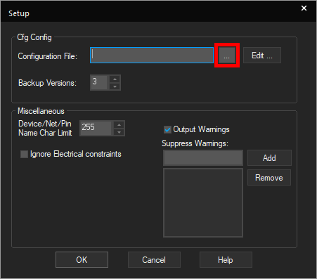
Step 7: The configuration file needs to be defined. Select the ellipsis.
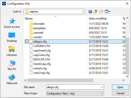
Step 8: Browse to the location of the allegro.cfg file. The default file path is: C:\Cadence\SPB_22.1\tools\capture.
Step 9: Select the file and click Open. Click OK in the Setup window.
Step 10: Click OK to netlist the design.
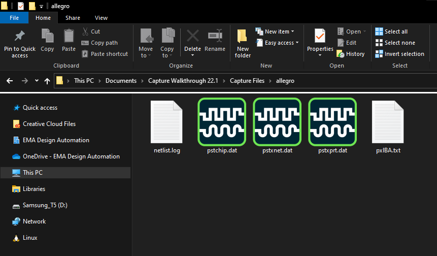
Note: The netlist files pstxnet.dat, pstxprt.dat, and pstchip.dat are generated in the specified location.
Creating the PCB Layout
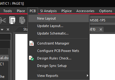
Step 11: To create a PCB layout, select PCB > New Layout from the menu. The New Layout window opens.
Step 12: Select the ellipses for PCB Layout Folder to open the file browser.
Step 13: Browse for a location for the board file to be saved. Click Select Folder.
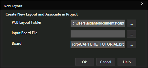
Step 14: In the Board field, enter a name for the board file.
Note: By default, this is the same as the project name.
Step 15: Leave Input Board File blank to create a new design.
Step 16: Click OK to create the new layout.
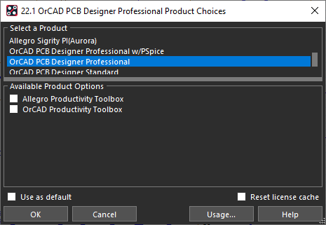
Step 17: The Cadence Allegro Product Choices window will open. Select OrCAD PCB Designer Professional from the list and click OK.
Note: This will open the new PCB layout file, which will be used in the PCB Walk-through.
Next Steps
This concludes the OrCAD Capture Walk-through. Continue learning OrCAD with the PCB Walk-through or PSpice Walk-through.