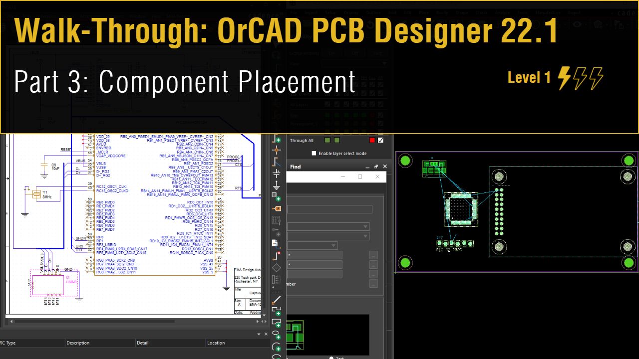
Lesson 3: Component Placement
This walk-through demonstrates several different options for placing components on your PCB in OrCAD PCB Designer 22.1 (2022). After you complete this topic, you will be able to:
- Place components
- Review a report that identifies unplaced components
- Cross probe components between Capture and PCB Editor
To follow along, continue with the design from the previous lesson or use the downloaded materials.
If materials were not downloaded at the start of the walk-through, they can be accessed in the Materials tab of this lesson.
 Open in New Window
Confirming Library Paths
Step 1: Select Setup > User Preferences from the menu.
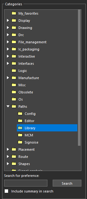
Step 2: In the Categories list, expand Paths and select Library.
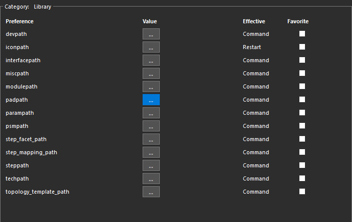
Step 3: Select the ellipsis for padpath to define the path for library padstacks.
Step 4: Ensure that C:/Cadence/SPB_22.1/share/pcb/pcb_lib/symbols is in the Directories list.
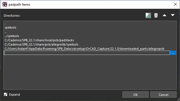
Note: If this entry is absent, select the Add button to add a new directory. Copy and paste the above file path into the text field and click OK.
Step 5: Select the ellipsis for psmpath to define the path for library symbols.
Step 6: Ensure that C:/Cadence/SPB_22.1/share/pcb/pcb_lib/symbols is in the Directories list.
Note: If this entry is absent, select the Add button to add a new directory. Copy and paste the above file path into the text field and click OK.
Step 7: Click OK to save the settings and close the User Preferences Editor.
Configuring Intertool Communication
Step 8: Open the provided capture_tutorial.dsn file in OrCAD Capture with PCB_TUTORIAL.brd in OrCAD PCB Designer. Set up a split-screen configuration.
Note: If your system has multiple monitors, you can put Capture in one monitor and PCB Designer in another.
Step 9: In Capture, select Options > Preferences from the menu.
Step 10: Select the Miscellaneous tab.
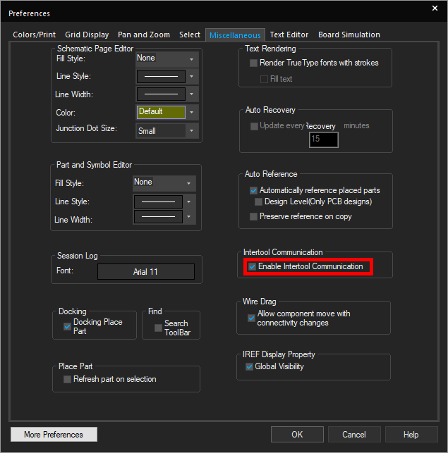
Step 11: Ensure the option for Enable Intertool Communication is checked. Click OK.
Placing Components from Capture
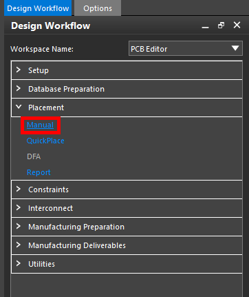
Step 12: In OrCAD PCB Designer, select Placement > Manual from the design workflow.
Note: This can be accessed in the menu by selecting Place > Components Manually.
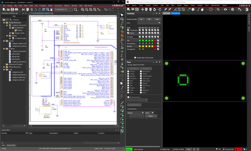
Step 13: Select IC1 in Capture.
Note: The component is attached to your cursor in PCB Designer.
Step 14: Click to place the component as shown above on the PCB. To rotate, right-click and select Rotate.
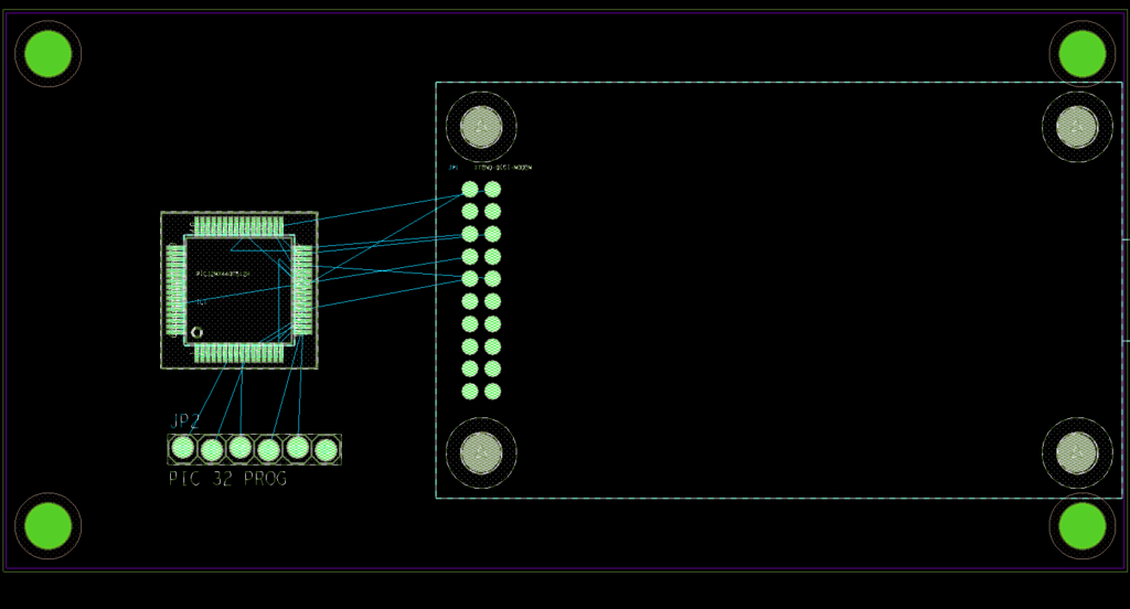
Step 15: Repeat this placement process for JP1 and JP2.
Note: Zoom into the canvas by scrolling the mouse wheel up. Zoom out by scrolling the wheel down.
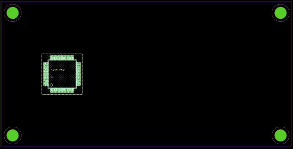
Step 16: In OrCAD Capture, select the USB connector, X1.
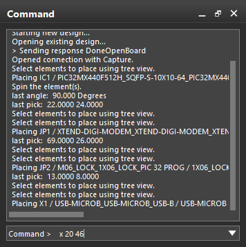
Step 17: In OrCAD PCB Editor, enter x 20 46 into the Command window and press Enter.
Note: If the Command window is not visible, select Display > Windows > Command from the menu. This move is required for proper integration with the mechanical enclosure.
Placing Components Manually
Step 18: Select Close in the Placement window.
Step 19: Expand OrCAD PCB Designer to a full screen. Select Placement > Manual from the Design Workflow.
Note: The already-placed components have been removed from the list.
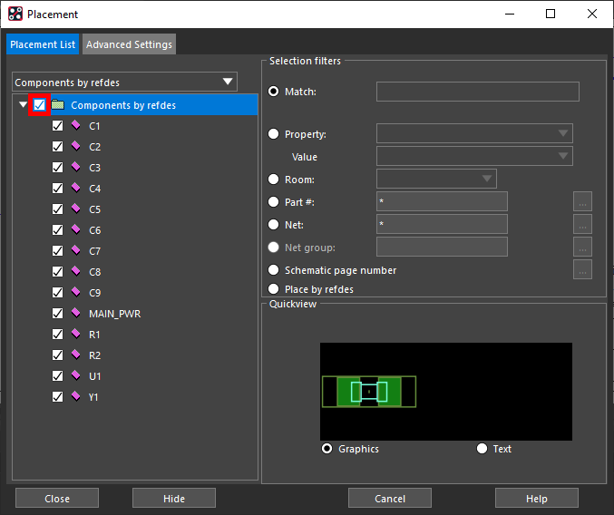
Step 20: Check the box for Components by refdes.
Note: This will select all components left to place.
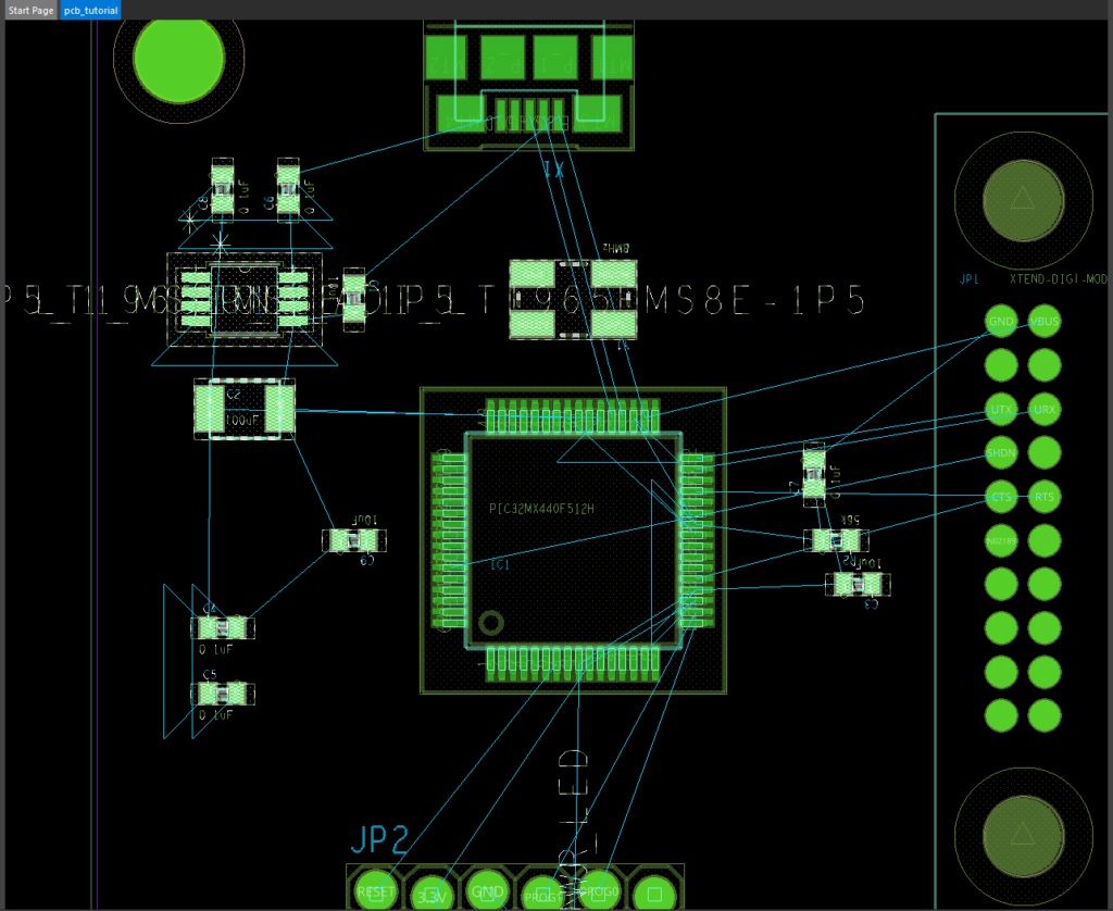
Step 21: Click to place the remaining components in the PCB canvas.
Note: Select Hide in the Placement window for better canvas visibility.
Step 22: When finished, select Close in the Placement window.
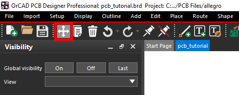
Note: If any components need to be moved, select the Move icon from the toolbar. Click the component then click to place it in the desired location on the PCB. Right-click and select Done.
Viewing the Placement
Step 23: Select Placement > Report in the Design Workflow.
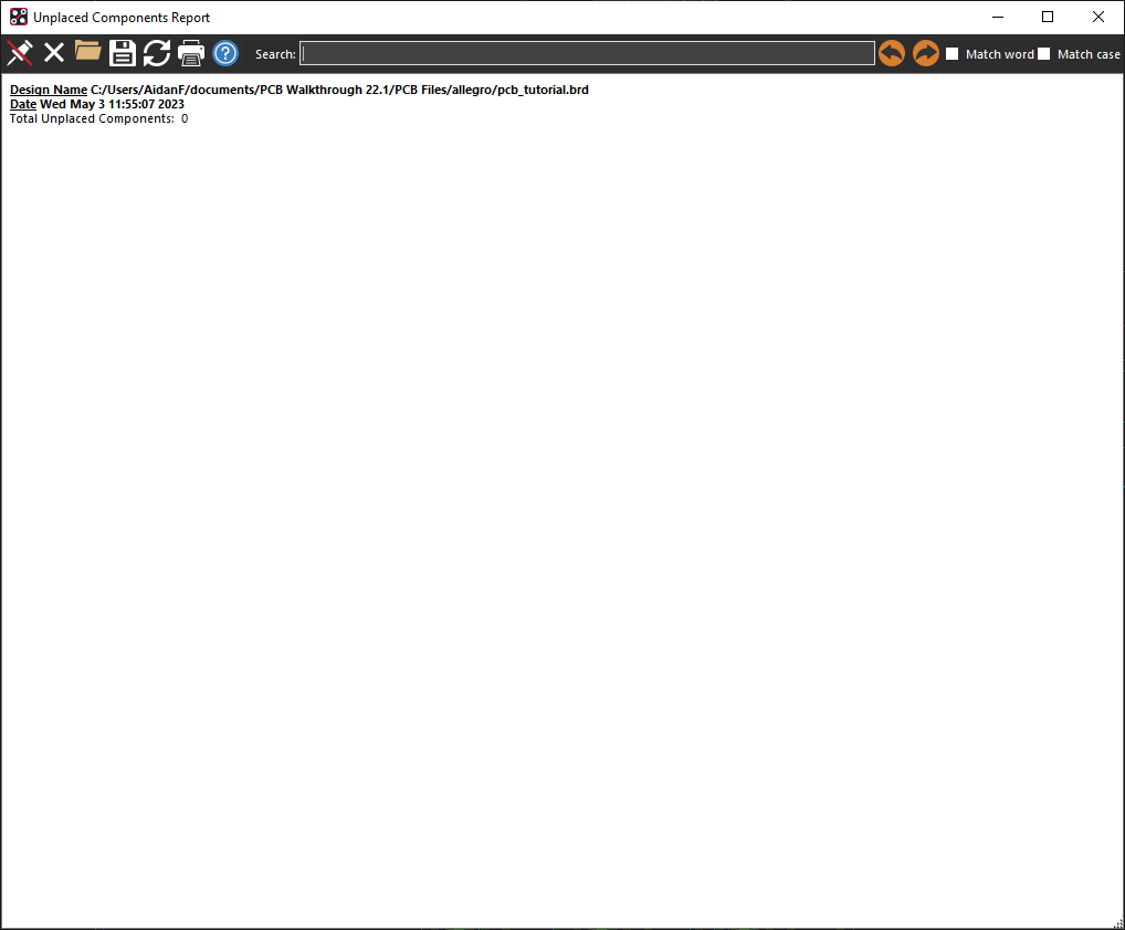
Step 24: View the Unplaced Component report.
Note: This will report any unplaced components.
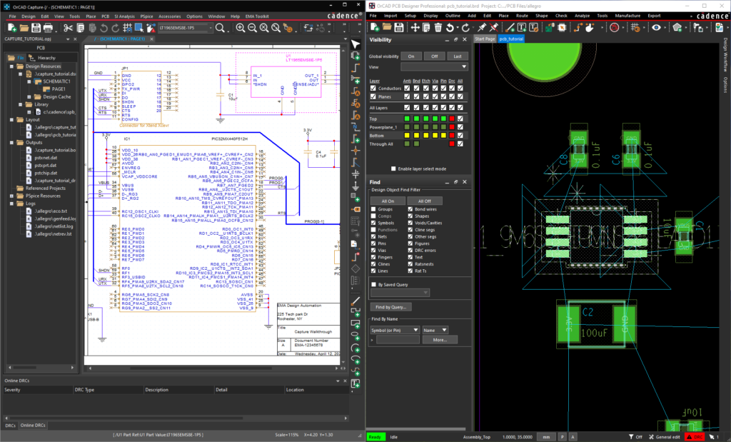
Step 25: Click a component in Capture to highlight its location in PCB Designer.
Step 26: Select a component in PCB Designer to be brought to the location in Capture.