Lesson 4: Constraints
This walk-through demonstrates how to set up differential pairs and constraints using OrCAD PCB Designer Professional 22.1 (2022). After you complete this topic, you will be able to:
- Set up a differential pair
- Specify electrical, physical, and differential pair rules with Constraint Sets
- Use Design Sync to communicate the required constraints
To follow along, continue with the design from the previous lesson or use the downloaded materials.
If materials were not downloaded at the start of the walk-through, they can be accessed in the Materials tab of this lesson.
 Open in New Window
Updating the Design Layout
Step 1: Open the provided capture_tutorial.dsn file in OrCAD Capture.
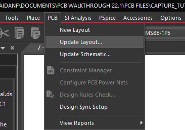
Step 2: Select PCB > Update Layout from the menu.
Step 3: Select Sync to open PCB Designer.
Note: This will enable a constraint driven design flow and sync the designs.
Step 4: Select the desired version of OrCAD PCB Designer from the software selection window.
Defining Differential Pairs
Note: If you defined differential pairs at the schematic level, skip ahead to Viewing Constraint Modes.
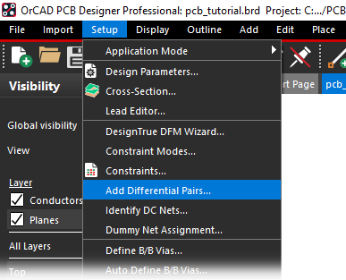
Step 5: In OrCAD PCB Designer, select Setup > Add Differential Pairs from the menu.
Step 6: Select Auto Generate.
Step 7: Enter DP_ for the DiffPair Name Prefix.
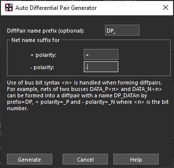
Step 8: Enter + for the + Polarity and – for the – Polarity.
Step 9: Select Generate.
Step 10: Click OK to close the window.
Viewing Constraint Modes
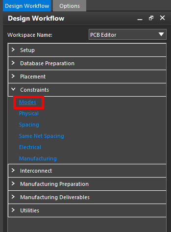
Step 11: Select Constraints > Modes from the Design Workflow.
Note: In the Modes window, select which constraints will be checked by setting the constraints On or Off.
Step 12: Ensure all constraints in the Physical list are configured as On.
Step 13: Select the Electrical list. Select On for All Differential Pair Checks to enable differential pair checks. Click OK to close the Analysis Modes window.
Defining Physical Constraints
Step 14: Select Constraints > Physical from the Design Workflow.
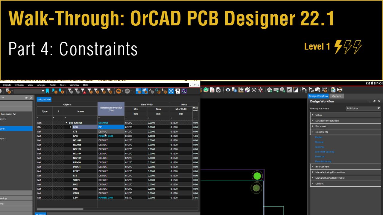
Note: This opens the constraint manager window. In the constraint manager, you can assign electrical, physical, spacing, and manufacturing constraints. Assign constraints by creating Constraint Sets (CSets) or assigning values to each individual net.
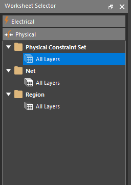
Step 15: In the Physical domain in the Constraint Manager, select the worksheet under Physical Constraint Set > All Layers.
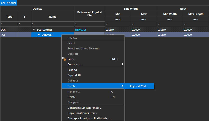
Step 16: Right-click the DEFAULT constraint set and select Create > Physical CSet.
Note: Constraint Sets (Csets) allow you to configure multiple rules as a group for efficient assignment to multiple nets.
Step 17: Enter POWER_GND for the name and click OK.
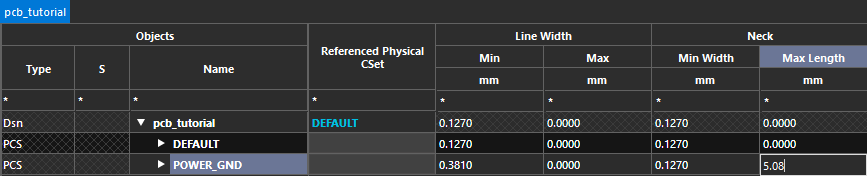
Step 18: Enter the following constraint values for the new CSet under their respective columns.
- Minimum line width: 0.381
- Minimum neck width: 0.127
- Maximum neck length: 5.08
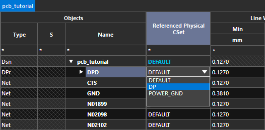
Step 19: Right-click the DEFAULT constraint set and select Create > Physical CSet.
Step 20: Enter DP for the name and click OK.
Note: This will create a group of rules for the differential pairs in the design.
Step 21: Enter the following constraint values for the new CSet under their respective columns.
- Minimum line width: 0.127
- Primary Gap: 0.127
Assigning Physical Constraints
Step 22: Select the Net > All Layers worksheet in the Physical domain.
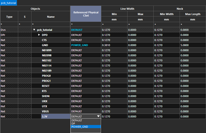
Step 23: Select the POWER_GND CSet from the dropdown in the Referenced Physical CSet column for 3.3V and GND.
Step 24: Select the DP CSet from the dropdown in the Referenced Physical CSet column for DPD.
Note: Assigning this CSet at the top level will assign it to each net of the differential pair.
Defining Electrical Constraints
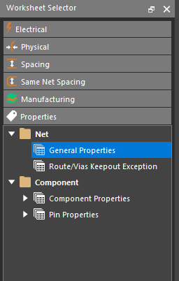
Step 25: Select the Electrical domain from the Worksheet Selector.
Note: Electrical constraints are available in OrCAD PCB Designer Professional.
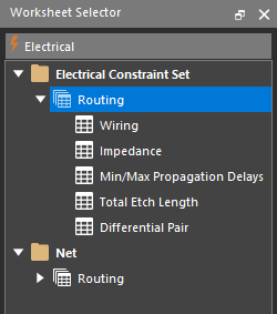
Step 26: Select the Electrical Constraint Set > Routing worksheet.
Step 27: Right-click in the table and select Create > Electrical CSet.
Step 28: Name the CSet DP and click OK.
Step 29: In the Worksheet Selector, select the Electrical Constraint Set > Routing > Differential Pair worksheet.
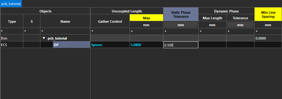
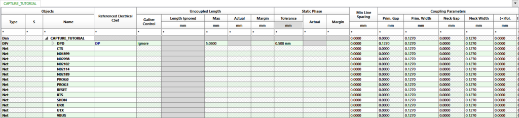
Step 30: Enter the following constraint values for the new CSet under their respective columns.
- Gather Control: Ignore
- Uncoupled Length: 5.08
- Static Phase Tolerance: 0.508
Step 31: Select the Net > Routing > Differential Pair worksheet.
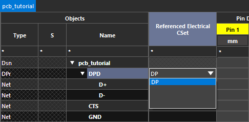
Step 32: Select the DP CSet from the dropdown in the Referenced Electrical Cset column for DPD.
Assigning Net Voltages
Step 33: Select the Properties domain in the Worksheet Selector.
Step 34: Select the Net > General Properties worksheet.
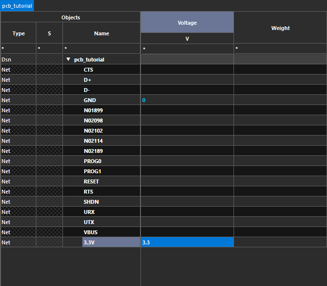
Step 35: In the Voltage column, assign 0 to GND and 3.3 to 3.3V.
Note: This will allow you to easily identify power and ground nets on the board and reduce the ratsnest.
Step 36: Close the Constraint Manager.
Syncing the Schematic
Step 37: Back in OrCAD Capture, select PCB > Update Schematic from the menu.
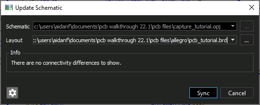
Step 38: The Update Schematic window opens. Select Sync.
Step 39: Select PCB > Constraint Manager from the menu.
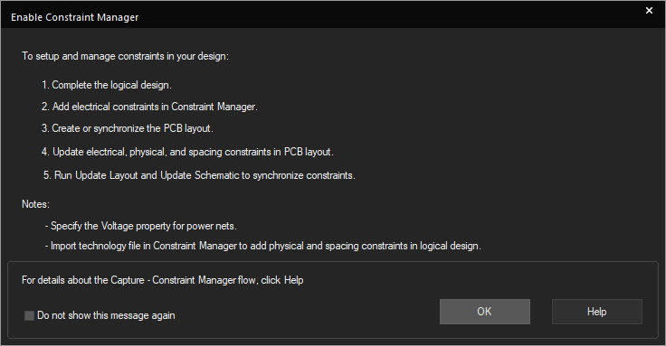
Step 40: The Enable Constraint Manager window opens. Click OK.
Step 41: View the Constraint Manager.
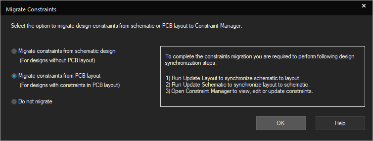
Note: If you see a window titled Migrate Constraints after clicking OK, the layout and schematic were not updated.
- Select Migrate constraints from PCB layout.
- Click OK.
- Select PCB > Update Layout.
- Click Sync.
- Select PCB > Update Schematic.
- Click Sync.
- Select PCB > Constraint Manager and try again.