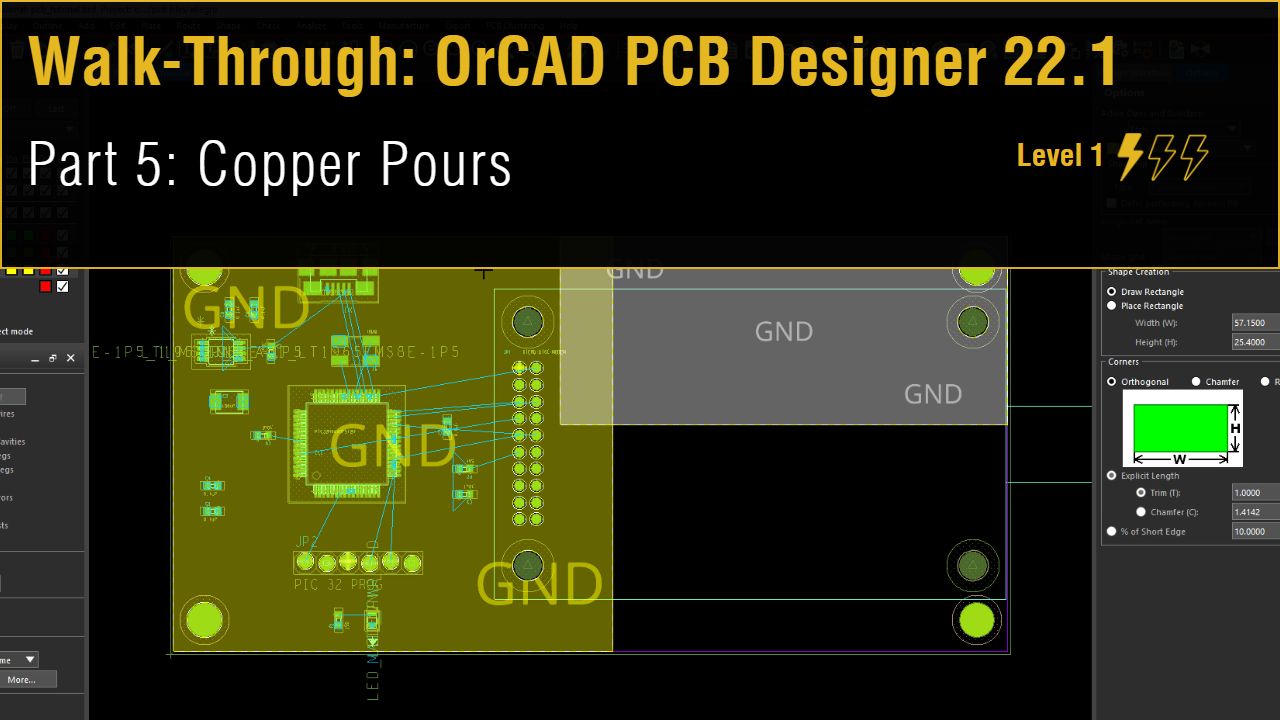
Lesson 5: Copper Pours
This walk-through demonstrates how create copper pours in OrCAD PCB Designer 22.1 (2022). After you complete this topic, you will be able to:
- Add ground and power planes
- Draw and merge geometric shapes
To follow along, continue with the design from the previous lesson or use the downloaded materials.
If materials were not downloaded at the start of the walk-through, they can be accessed in the Materials tab of this lesson.
 Open in New Window
Drawing a Rectangular Shape
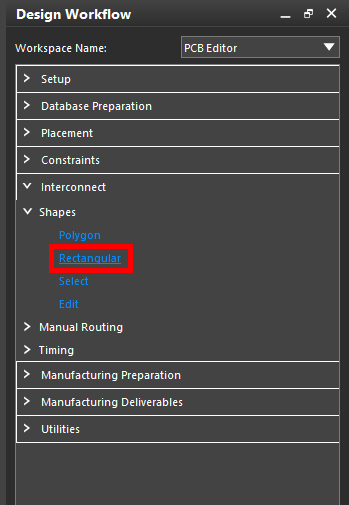
Step 1: Expand the Interconnect category in the Design Workflow. Select Shapes > Rectangular.
Step 2: Select the Options tab.
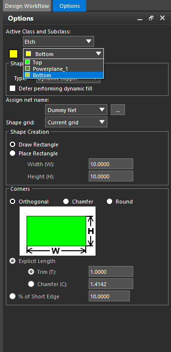
Step 3: Select Etch from the Active Class drop-down menu and Bottom from the Active Subclass dropdown.
Step 4: Select GND from the dropdown under Assign Net Name.
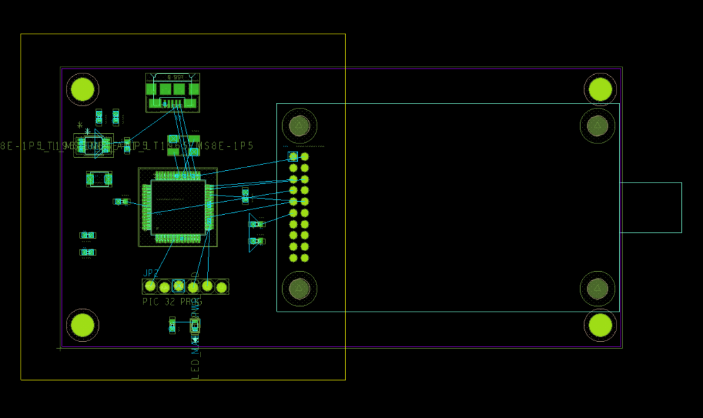
Step 5: Click to start drawing a rectangle. Draw the rectangle over half the board. Click again to finish the drawing.
Step 6: Draw an overlapping rectangle over half of the remaining empty space in the board. Right-click and select Done.
Merging the Shapes
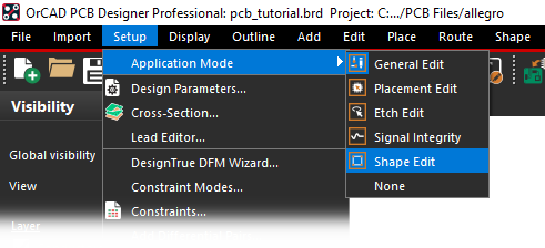
Step 7: Select Setup > Application Mode > Shape Edit from the menu.
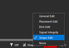
Note: Alternatively, you can change the application mode by selecting the wrench/screwdriver icon in the bottom-right corner of the screen and select the desired mode from the resulting pop-up menu.
Step 8: Right-click either of the shapes and select Merge Shapes.
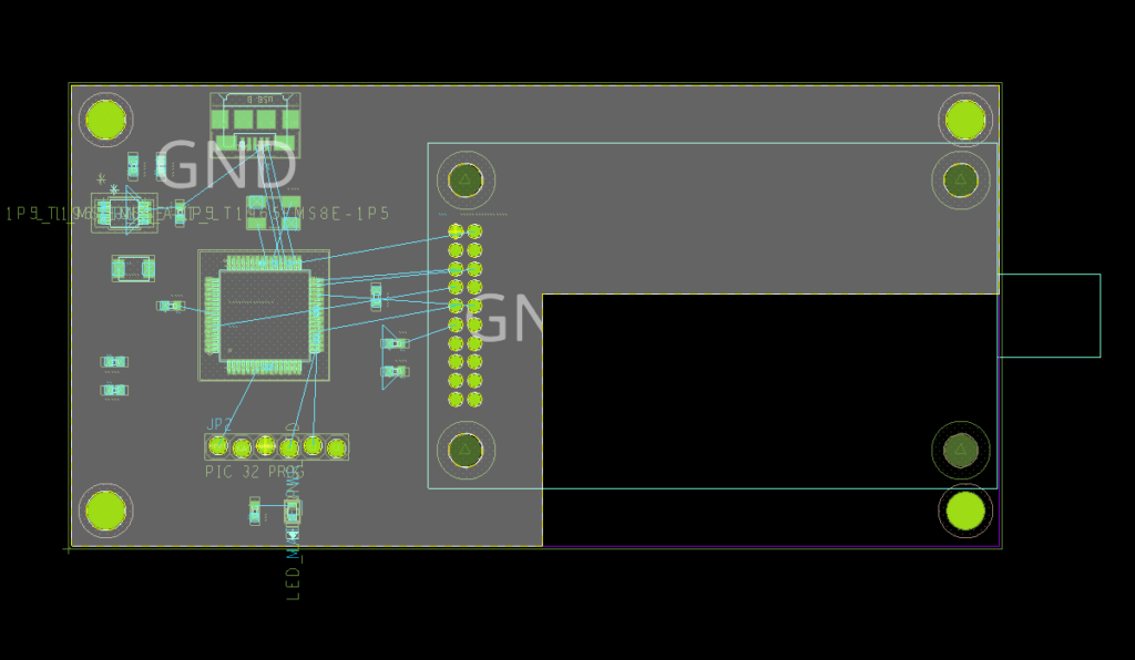
Step 9: Click the other shape. The shapes have been merged into one.
Drawing a Polygon
Step 10: In the Design Workflow, select Interconnect > Shapes > Polygon.
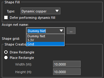
Step 11: In the Options tab, select GND from the Assign Net Name dropdown.
Step 12: Click to place the first corner of the polygon.
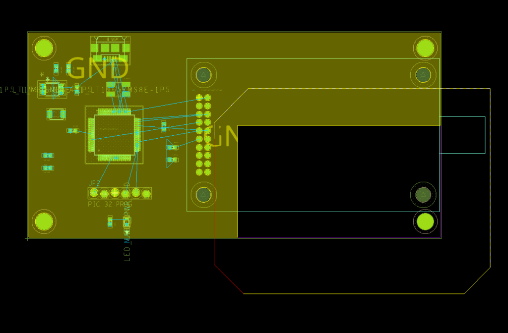
Step 13: Draw the polygon over the remainder of the board.
Step 14: When all sides of the polygon are complete except the last connection, right-click and select Complete.
Note: This will automatically finish the final connection and complete the polygon shape.
Step 15: Right-click and select Done.
Step 16: Right-click the polygon and select Merge Shapes.
Step 17: Select the merged rectangular shapes to add the polygon.
Creating a Full Copper Pour
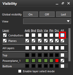
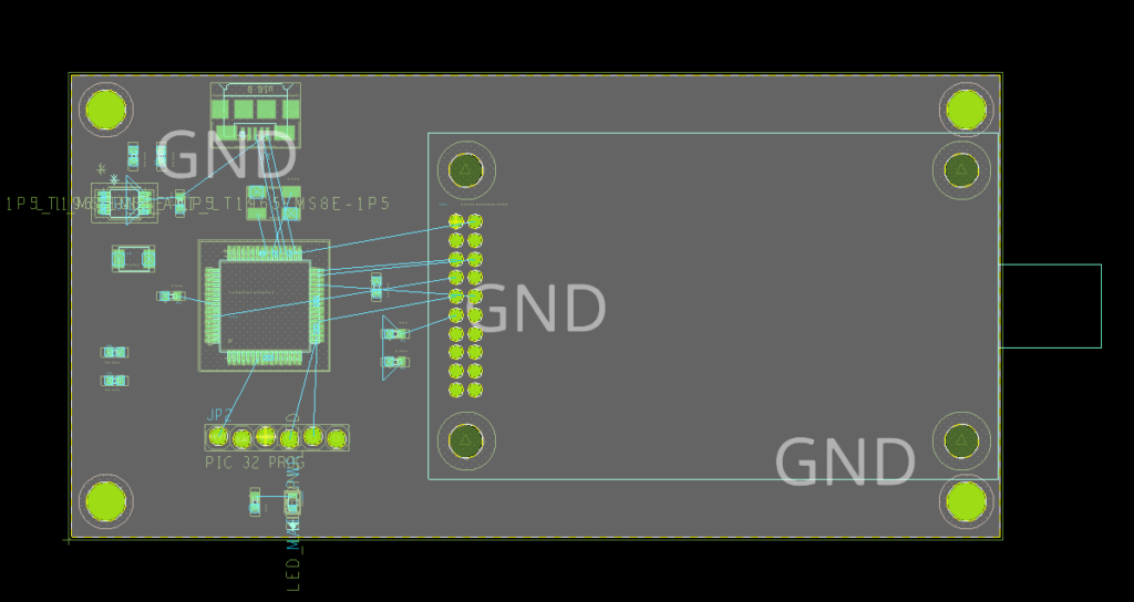
Step 18: In the Visibility panel, un-check the All checkbox for Conductors to turn off conductor visibility.
Step 19: Select Edit > Split Plane from the menu.
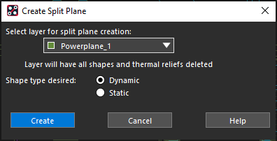
Step 20: Select Powerplane_1 from the drop-down menu and click Create.
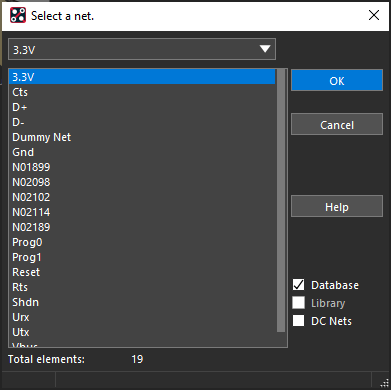
Step 21: The Select a Net window opens. Select 3.3V from the list and click OK.