Lesson 6: Part Information
This walk-through demonstrates how you can add and edit design part information either before or after part placement in OrCAD Capture version 22.1 (2022). After you complete this topic, you will be able to:
- Edit component values and display information on the schematic
- Add PCB footprints to your design
To follow along, continue with the design from the last topic or use the provided design files. If the design files were not downloaded in the beginning of the Capture Walk-Through, the design files for this lesson can be found under the Materials tab.
 Open in New Window
Assigning Power Net Values
Step 1: Hold the CTRL key and select all four VCC components in the schematic.
Note: If you accidentally select something else, click it again while holding CTRL to de-select it.
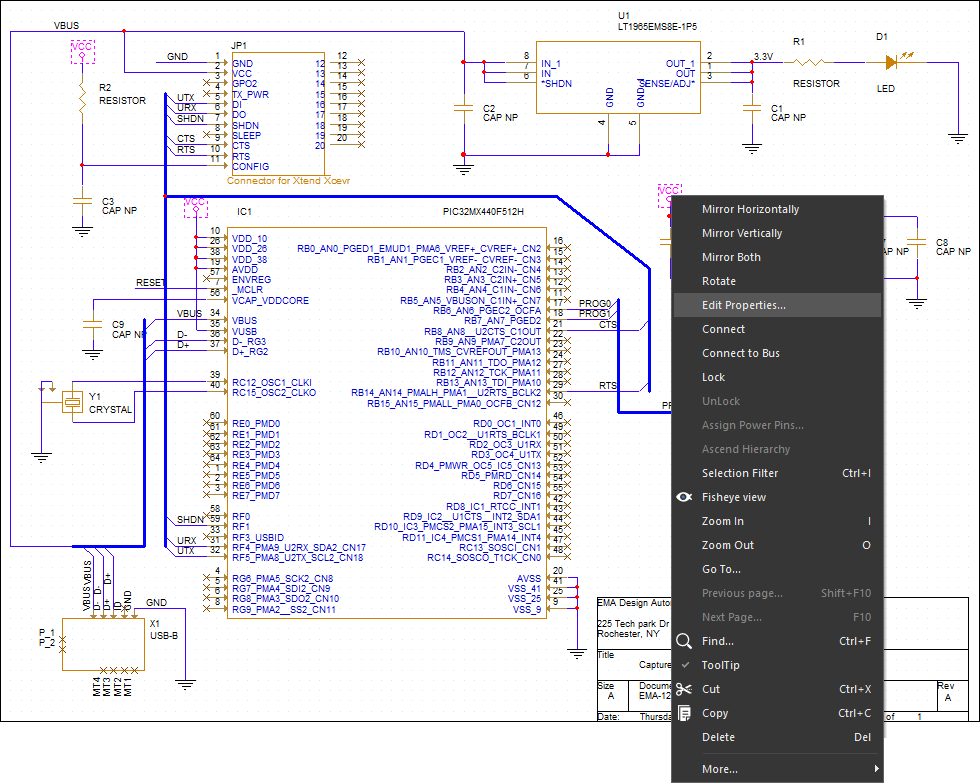
Step 2: Right-click on any of the selected components and select Edit Properties.
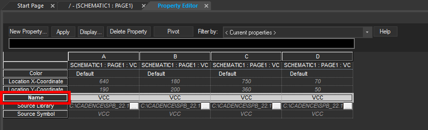
Step 3: The Property Editor tab opens. Select the Name row.
Step 4: Right-click and select Edit.
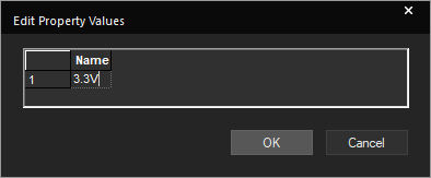
Step 5: Enter 3.3V into the Name cell and click OK.
Note: The name has been assigned to all VCC symbols and will connect them to the net with alias 3.3V.
Step 6: Close the Property Editor tab.
Note: You can also assign the value during placement. Select Place > Power from the menu. Select VCC and OK. Before placing, right click and select Edit Properties. Add 3.3V for the value and click OK. Now the component will be placed with the correct value.
Defining Component Values
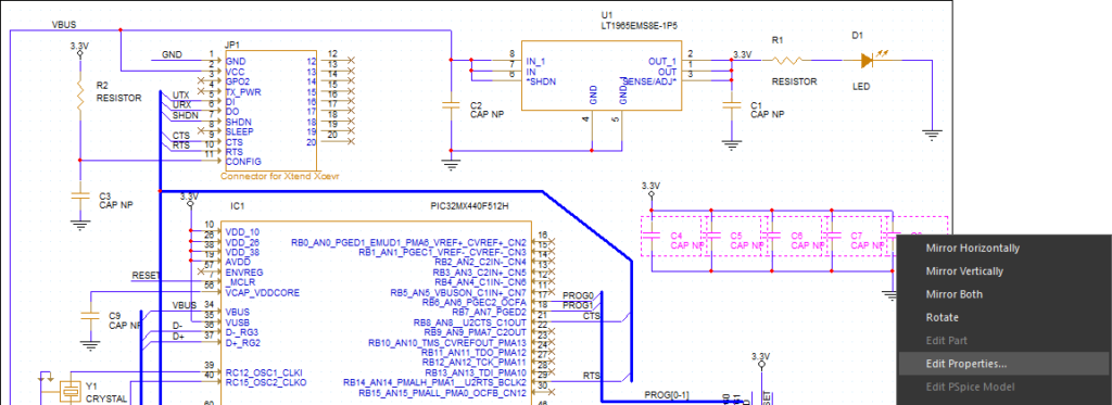
Step 7: Hold CTRL and click to select the row of parallel capacitors. Right-click and select Edit Properties.
Step 8: Select the Value row. Right-click and select Edit.
Step 9: Enter a value of 0.1uF and click OK.
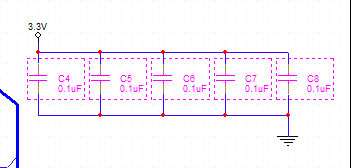
Step 10: Close the Property Editor tab. The capacitor values have been updated.
Note: You can also activate the properties window by double clicking a component. You can change the Display Format in the Display Properties window.
Step 11: Hold CTRL and select capacitors C2, C3, and C9. Right-click and select Edit Properties.
Step 12: Select the Value row. Right-click and select Edit.
Step 13: Enter a value of 10uF and click OK. Close the Property Editor tab.
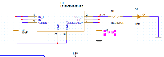
Step 14: Double-click the value (CAP NP) of capacitor C1 to change it.
Step 15: Enter 100uF for the value and click OK.
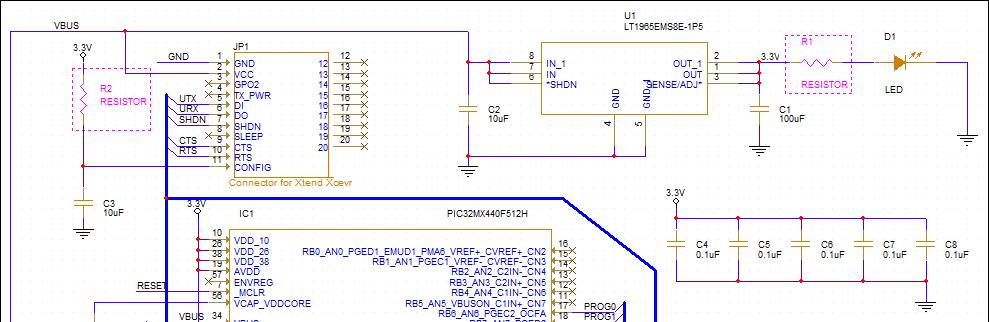
Step 16: Hold CTRL and select resistors R1 and R2. Right-click and select Edit Properties.
Step 17: Double-click the Value cell for R1 and enter a value of 150. Double-click the Value cell for R2 and enter a value of 56k. Close the Property Editor tab.
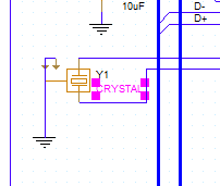
Step 18: Double-click the value for crystal Y1.
Step 19: Enter a value of 8MHz and click OK.
Changing the Color Value
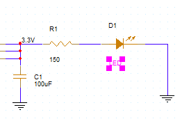
Step 20: Double-click the value for LED D1.
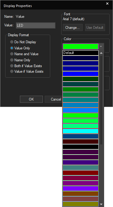
Step 21: Select green from the Color drop-down menu in the Display Properties window.
Step 22: Click OK. The color of the LED value has been changed to green.
Defining Footprints
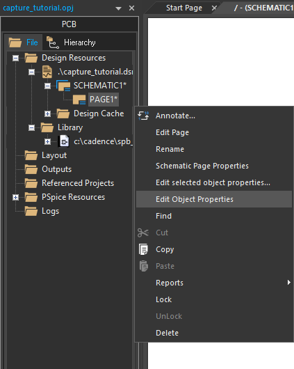
Step 23: In the project hierarchy, select PAGE1, right-click and select Edit Object Properties.
Note: This will display the properties for all the components placed on Page 1 of the schematic. Footprints have not been assigned for capacitors, resistors, or the LED. The footprint for the part placed through Ultra Librarian was automatically assigned.
Step 24: Enter 1210 into the cell on the PCB Footprint row under C1 to assign the footprint.
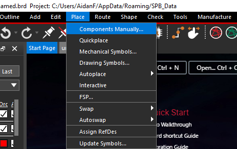
Note: If the footprint name is unknown, open OrCAD PCB Designer. Select Place > Components Manually from the menu.
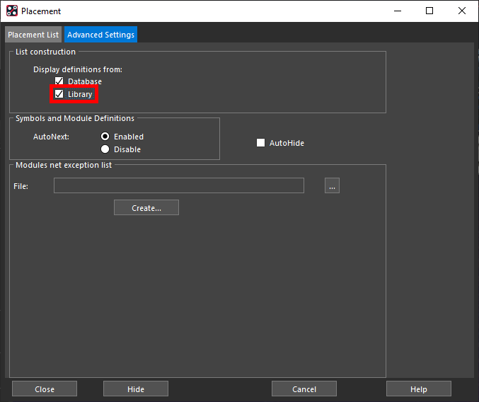
Select the Advanced Settings tab and check Library.
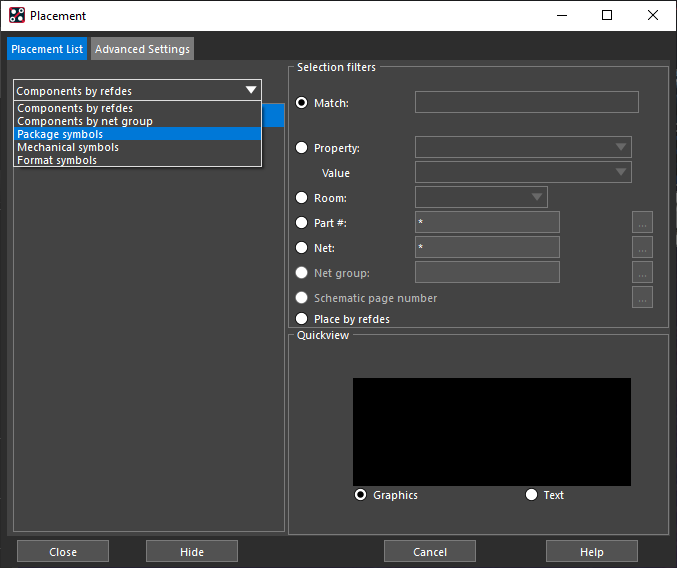
Return to the Placement List tab and select Package Symbols from the drop-down menu.
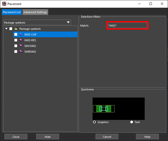
Search for *0402* and press Enter on the keyboard. This will return any footprint with 0402 in the name. Check the box next to the name to preview the 0402-CAP footprint.
Step 25: Enter 0402-CAP into the cell on the PCB Footprint row under C2 to assign the footprint.
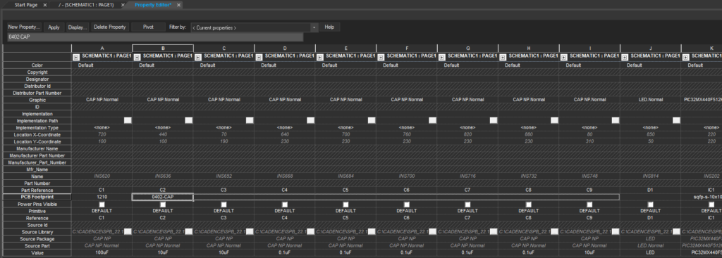
Step 26: Click and drag the marker to extend the footprint to C3-C9.
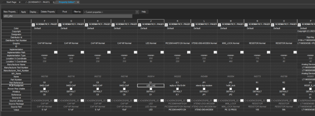
Step 27: Enter LED_LNJ into the cell on the PCB Footprint row under D1 to assign the footprint to the LED.
Step 28: Enter 0402-RES into the cell on the PCB Footprint row under R1 and R2 to assign the footprints.
Note: You can use the keyboard shortcuts CTRL-C and CTRL-V.
Step 29: Close the Property Editor tab.
Step 30: Back in the schematic, right-click a component and select Show Footprint.
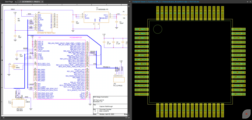
Step 31: Verify the footprint in the Footprint Viewer.