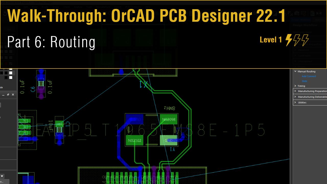
Lesson 6: Routing
This walk-through demonstrates how to route the PCB in OrCAD PCB Designer 22.1 (2022). After you complete this topic, you will be able to:
- Route and clean-up traces
- Verify all nets are routed
To follow along, continue with the design from the previous lesson or use the downloaded materials.
If materials were not downloaded at the start of the walk-through, they can be accessed in the Materials tab of this lesson.
 Open in New Window
Adjusting Net Colors
Step 1: Select Setup > Colors from the menu or the Color192 icon from the toolbar.
Note: This is also accessible through the design workflow.
Step 2: Select the All checkbox twice to turn off visibility for all layers.
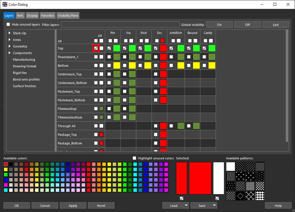
Step 3: Select the All checkbox for Top to enable visibility for the top layer.
Step 4: Select the Nets tab.
Note: This will allow you to set colors by nets.
Step 5: Select Purple from the palette of available colors.
Step 6: Select the cell under the Net column for 3.3V.
Step 7: Select Blue from the palette of available colors.
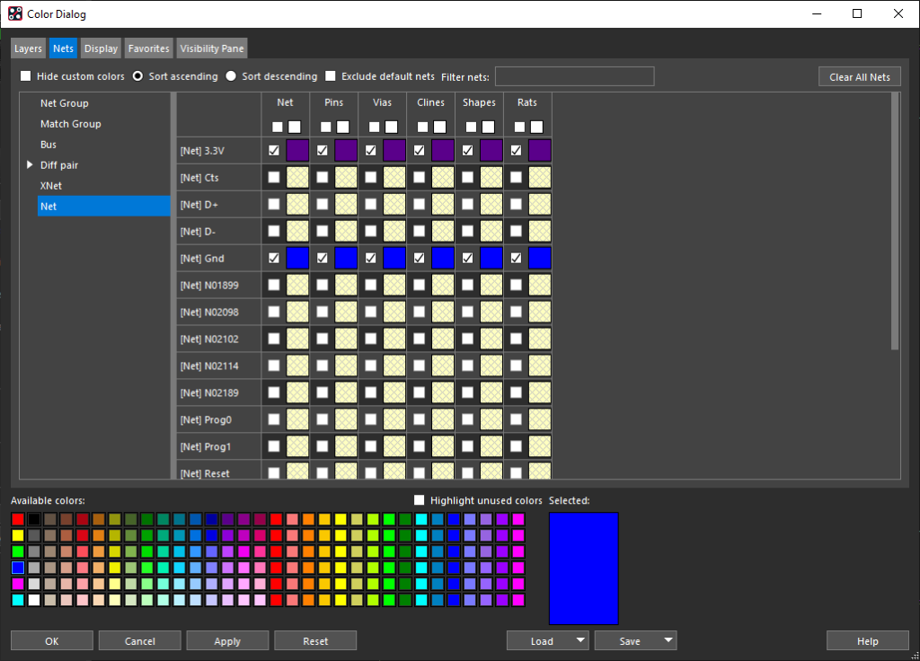
Step 8: Select the cell under the Net column for GND.
Step 9: Click OK to save the settings and close the Color Dialog window.
Creating Fanouts
Step 10: Select Route > Create Fanout from the menu.
Step 11: In the Find panel, select All On.
Note: This will allow you to select both Pins and Symbols for fanout creation. If the Find panel is not visible, select Display > Windows > Find from the menu.
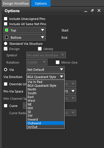
Step 12: In the Options panel, select Outward from the Via Direction dropdown.
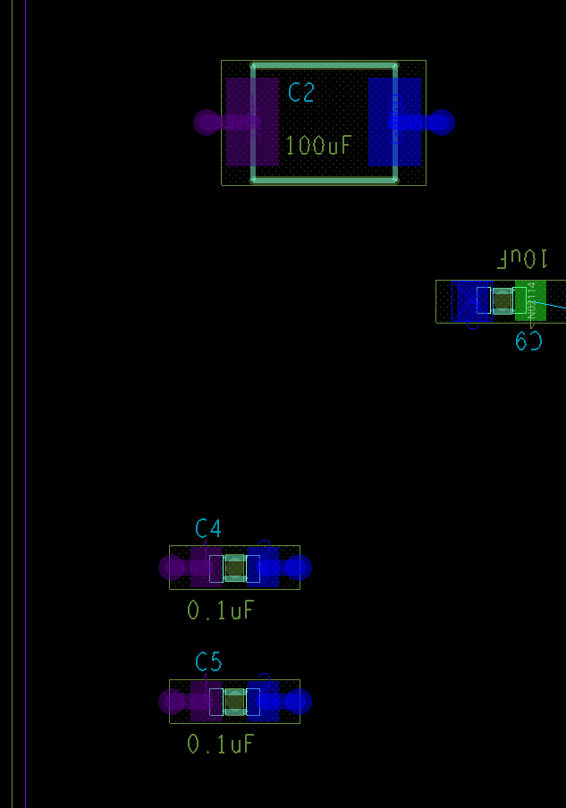
Step 13: Select all components with both pins connected to either ground or power.
Note: When completed, fanouts for six components should be completed. Net colors assigned in the previous section make identification easy.
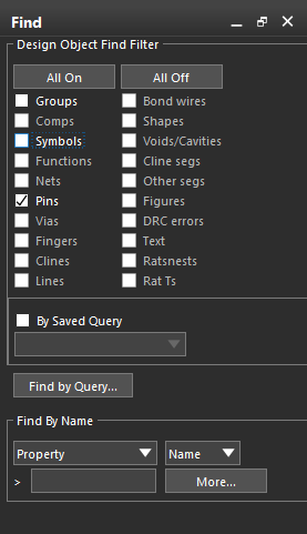
Step 14: In the Find panel, un-check Symbols.
Note: This will select and fan out only individual pins.
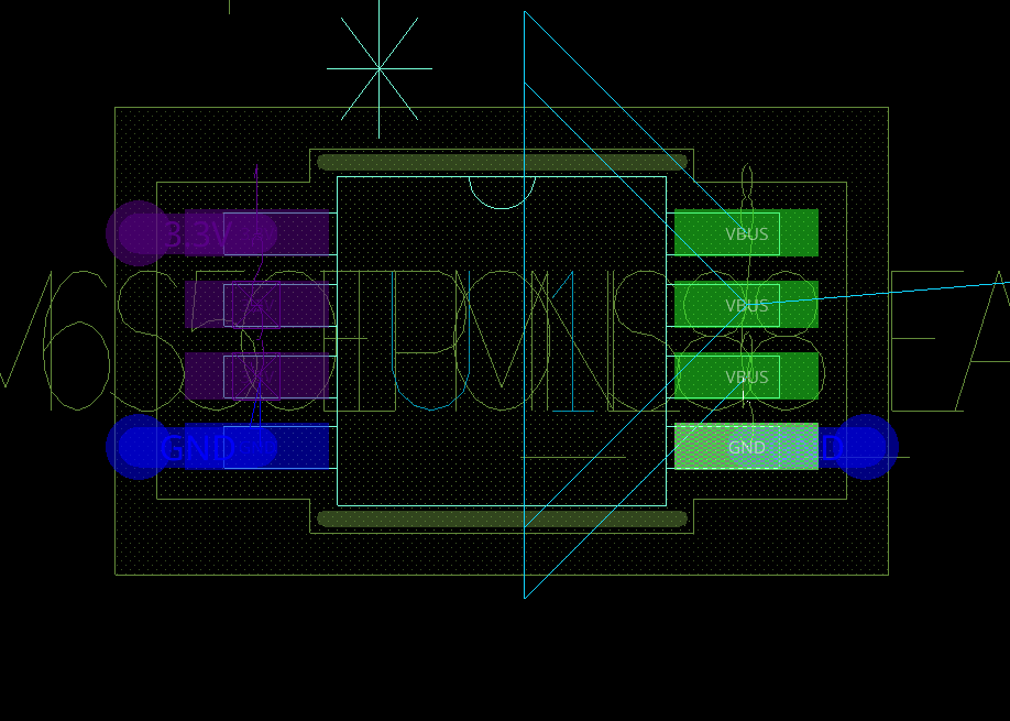
Step 15: Click both ground pins and one of the power pins on U1.
Note: The remainder of the power pins will be connected to each other, so only one pin needs to be fanned out.
Step 16: Click the remaining power and ground pins, except those on Crystal Y1, to create the fanouts. Right-click and select Done when finished.
Note: When completed, there should be 19 individual pins fanned out. There is no need to fan out any through-hole power or ground pins, such as those on JP1 and JP2. Some fanouts are in violation of the configured design rules. These errors will be resolved in the next topic of the walk-through.
Routing Traces
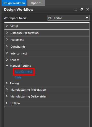
Step 17: In the Design Workflow, select Interconnect > Manual Routing > Add Connect.
Note: Alternatively, select Route > Connect from the menu or the Connect button from the toolbar.
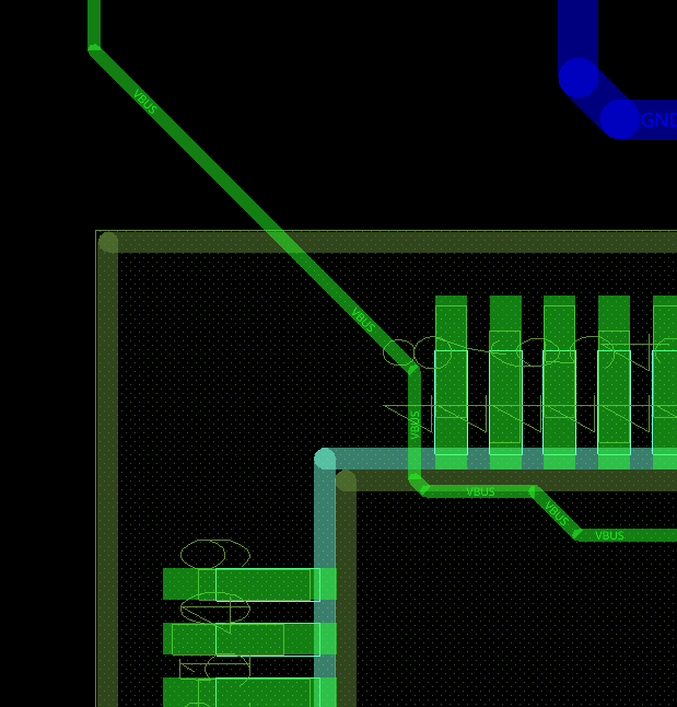
Step 18: Select one of the differential pair nets on the USB connector.
Note: Both nets of the differential pair have been activated and will be routed together according to the rules defined in the constraint manager.
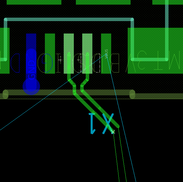
Step 19: Click to place a trace and click the corresponding connection on IC1 to finish routing the differential pair traces.
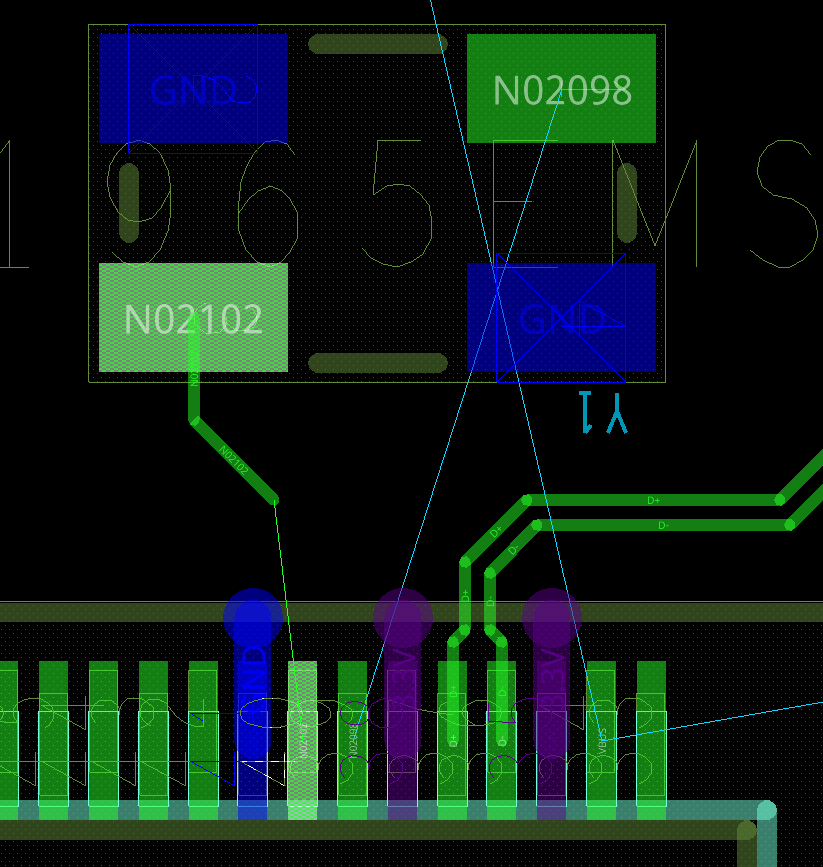
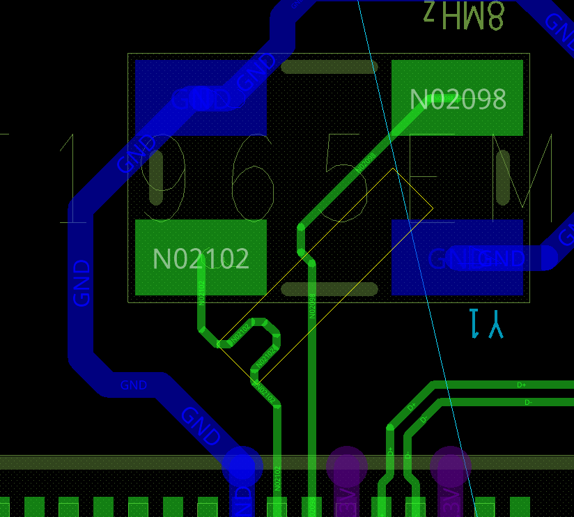
Step 20: Select net N02102 on Y1. Click the canvas to place the trace.
Step 21: Click the corresponding pad on IC1 to finish the trace.
Step 22: Select net N02098 on Y1. Click the canvas to place the trace. Click the corresponding pad on IC1 to finish the trace.
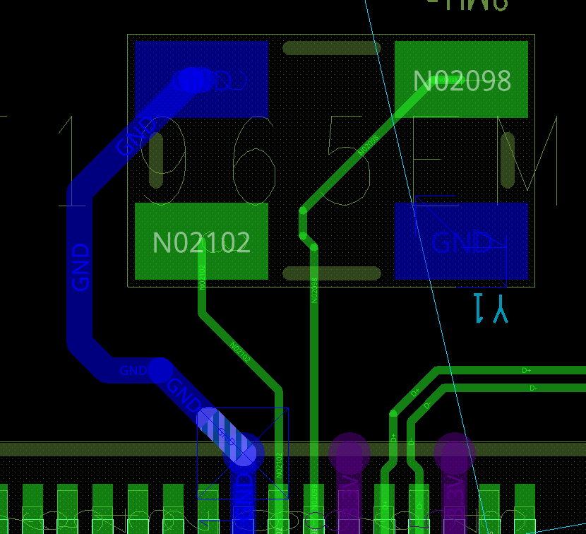
Step 23: Select the first unrouted ground pin on Y1. Click the canvas to place the trace and click the fanout via from IC1 to complete the connection.
Step 24: Select the second unrouted ground pin on Y1. Click the canvas to place the trace and complete the connection to the first ground.
Delay Tuning in OrCAD
Step 25: Select Route > Delay Tune from the menu.
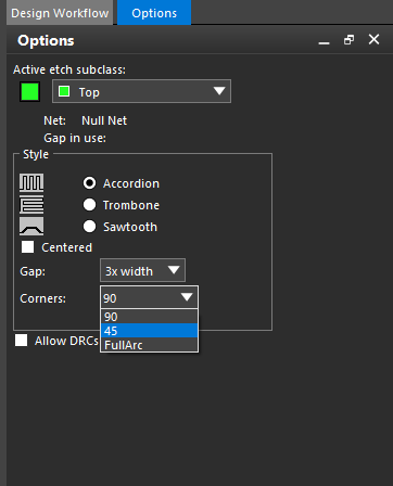
Step 26: In the Options panel, set the Gap to 3x Width and the Corners to 45.
Step 27: Select the shorter of the previously routed connections between Y1 and IC1.
Step 28: Move the cursor away from the trace to add delay tuning to even out the lengths of the two nets.
Step 29: When finished, right-click and select Done.
Step 30: Click to select the whole trace. Right-click and select Fix.
Note: This will lock the trace and prevent it from being edited.
Step 31: Click to select the other traces connected to Y1. Right-click and select Fix.
Routing the Remaining Traces
Step 32: Select Interconnect > Manual Routing > Add Connect from the Design Workflow or Route > Connect from the menu.
Step 33: Beginning routing the connections on the PCB.
Note: In the Options tab, you can set:
- the angle of the trace
- change the line width
- choose to shove or hug a trace, shove vias, smooth traces
- auto blank all other rats
Step 34: Complete all the connections on the PCB.
Note: Once a net has been selected, the ratsnest line will show where the net should be connected. If you make mistake while routing, right-click and select Oops.
Step 35: When finished, right-click and select Done.
Smoothing Traces in the Design
Note: The design can be smoothed manually with the Slide command or automatically with Custom Smooth.
Step 36: Select Interconnect > Manual Routing > Slide from the Design Workflow or Route > Slide from the menu.
Step 37: Click the segment you want to slide and click again to place it.
Step 38: Select Route > Custom Smooth from the menu.
Step 39: Click and drag to highlight the entire design to apply smoothing to all the traces. Right-click and select Done when finished.
Checking the Connections
Step 40: Select Utilities > Display Status from the Design Workflow.
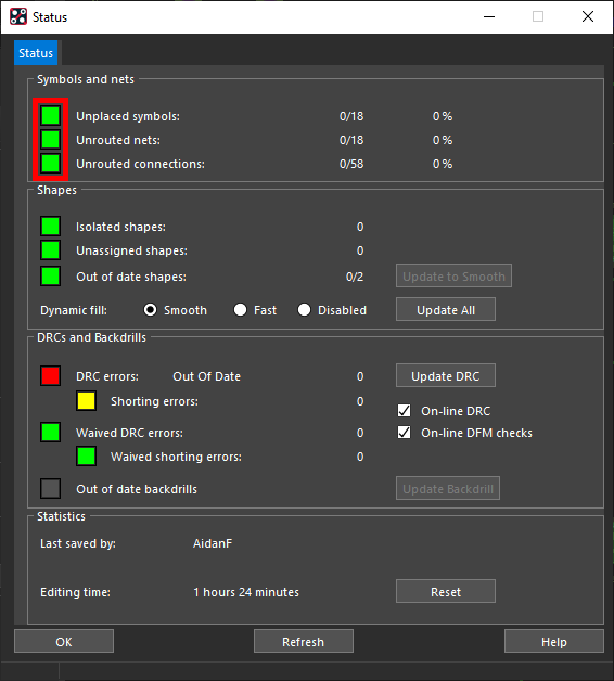
Step 41: Ensure that all nets and connections are routed, as indicated by green buttons.
Note: If all nets and connections are routed, the corresponding buttons will be color-coded green. If any nets or connections are unrouted, the corresponding buttons will be color-coded yellow. To resolve the unrouted connections, use the following steps:
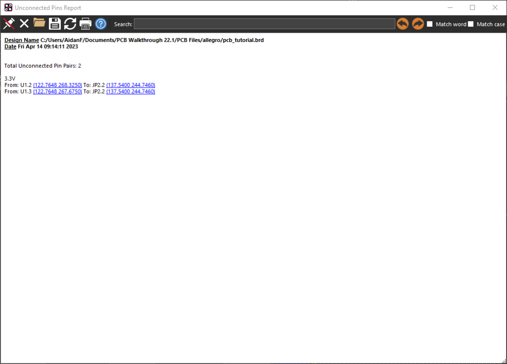
- Select the button next to Unrouted Connections. This will activate the Unconnected Pins Report, which displays the pin pairs that are not connected.
- Select a coordinate to be brought to the location on the PCB.
- Close the Display Status window.
- Route the unrouted connection(s).
- Select Utilities > Display Status from the Design Workflow to confirm all nets and connections are routed.