Lesson 7: Design Rule Check (DRC)
This walk-through conducts a final design rule check (DRC) in OrCAD PCB Designer 22.1 (2022) which is necessary to prepare the board for manufacturing. After you complete this topic, you will be able to:
- Run a Design Rule Check
- Check the status of a design
- Use the DRC Browser
- Identify and correct DRC errors
To follow along, continue with the design from the previous lesson or use the downloaded materials.
If materials were not downloaded at the start of the walk-through, they can be accessed in the Materials tab of this lesson.
 Open in New Window
Checking for DRC Errors
Step 1: Select Utilities > Display Status from the Design Workflow.
Note: Alternatively, select Check > Design Status from the menu.
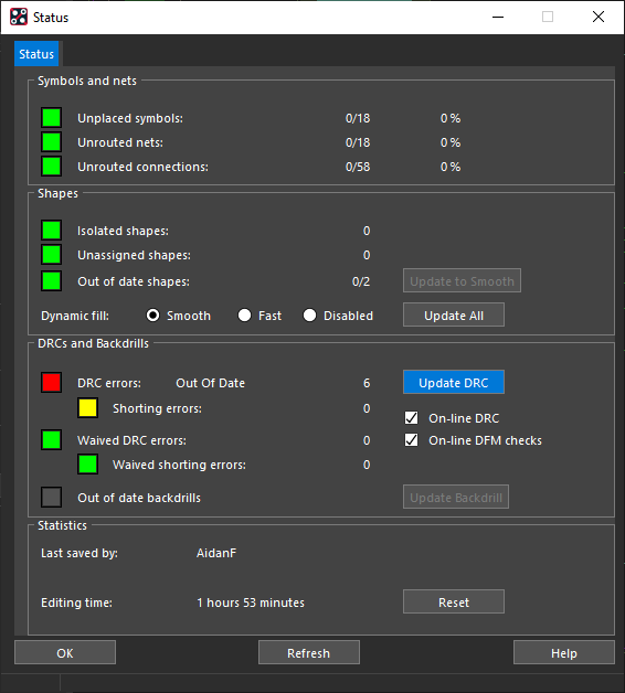
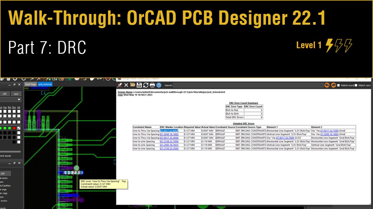
Step 2: The button next to DRC Errors is red, indicating that the DRC cache is out of date. Select Update DRC.
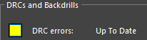
Step 3: The button next to DRC Errors is now yellow, indicating that an error has been detected. Click the button to view the DRC report.
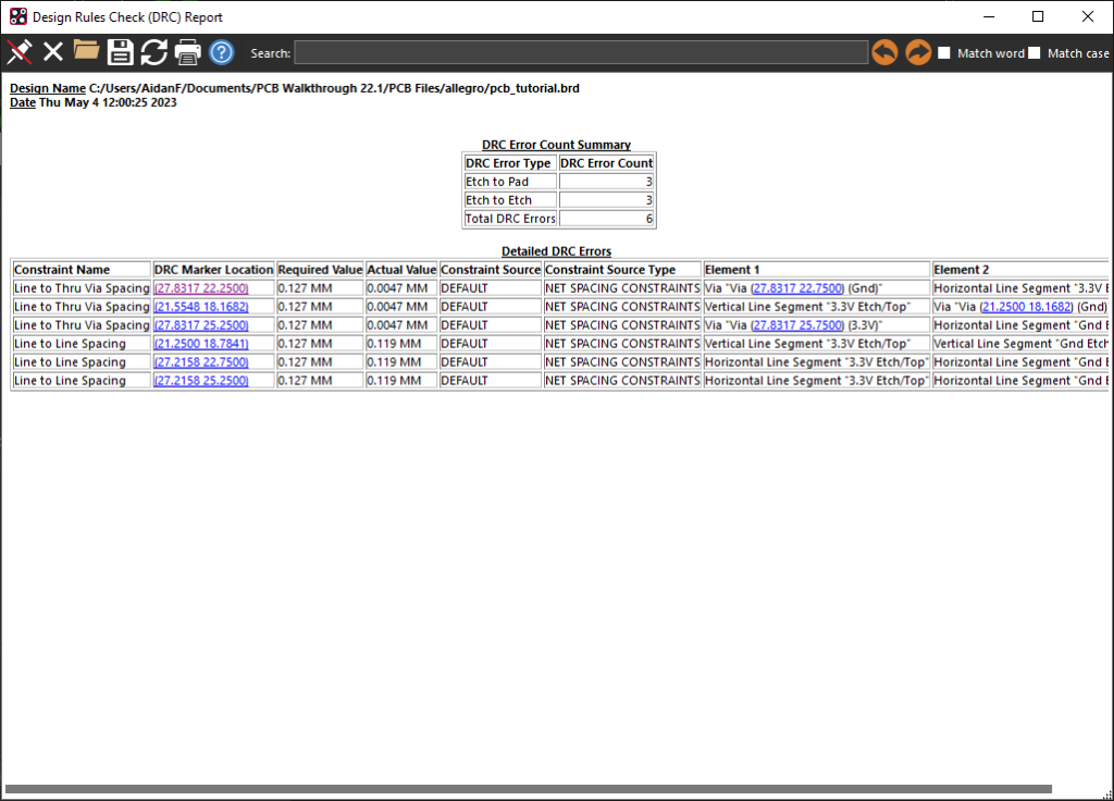
Step 4: The DRC report opens, showing the total count for each error type and a list of errors. Select the coordinates for one of the DRC markers for Line to Thru Via Spacing to be brought to the location of the error on the PCB.
Note: This table also lists the constraint set in violation, the constraint source type, and the elements involved. Additional errors may be present depending on how the design was routed. Adjust traces in the design as required to correct DRC errors.
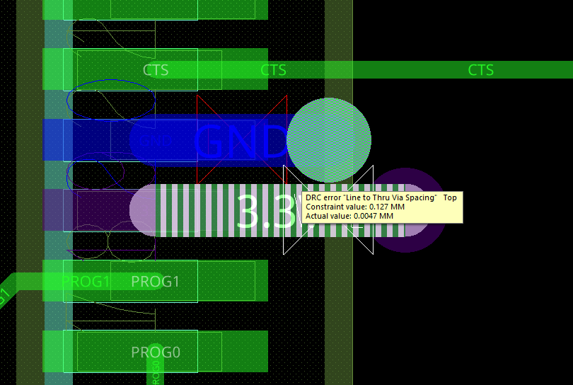
Step 5: Hover your cursor over the marker for additional information. This error was caused by the power and ground fanouts on IC1 being too close together.
Note: By hovering over the marker additional information can be reviewed on the DRC. This error reports that trace to trace spacing must be greater than 0.127mm when the actual value is 0.0047mm.
Step 6: Close the report and Status window.
Correcting Spacing Errors
Step 7: Select Setup > Application Mode > Etch Edit from the menu.
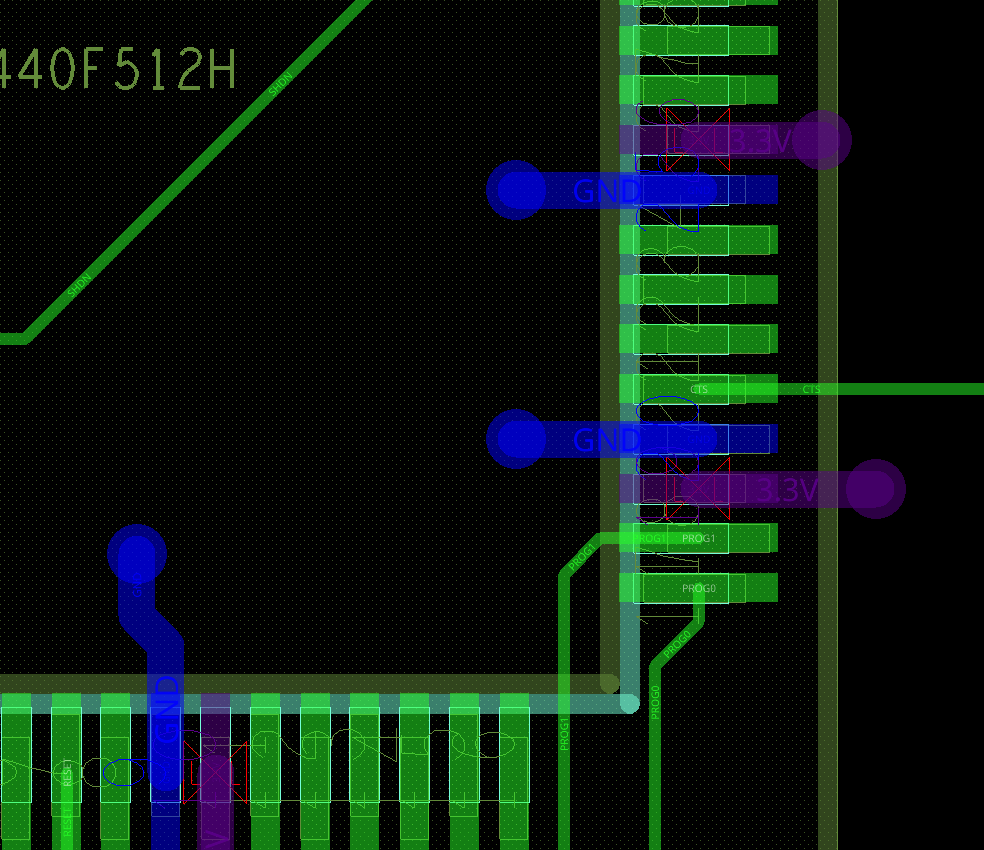
Step 8: Click and drag the ground vias on the bottom and side of IC1 to move them to the inside of the chip.
Note: The DRC errors are resolved and the markers are removed.
Viewing the DRC Browser
Step 9: Select Utilities > DRC Browser from the Design Workflow.
Note: Alternatively, select Tools > DRC Browser from the menu.
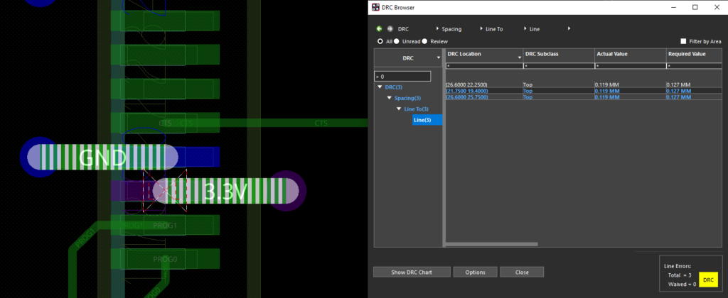
Step 10: Here you can view all DRC errors on the board and browse by category. Expand the categories and select the coordinates of the error to be brought to its location on the PCB and zoomed in.
Step 11: Select Line To in the DRC list.
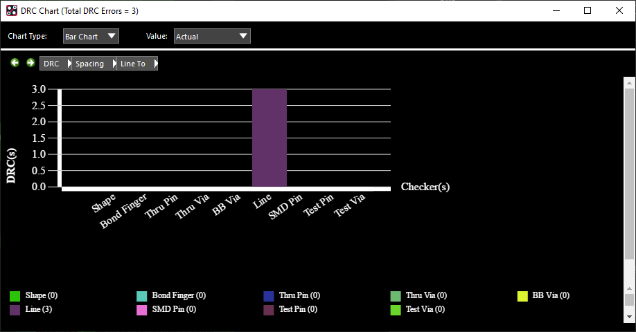
Step 12: Select Show DRC Chart to open the DRC chart. The DRC chart shows a graphical representation of how many of each type of error are present.
Step 13: Close the DRC chart.
Correcting DRC Errors
Step 14: Select Edit > Change Objects from the menu.
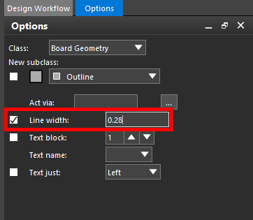
Step 15: In the Options panel, check the option for Line Width. Set the Line Width value to 0.28.
Step 16: Click the erroneous traces to change them to 0.28mm wide.
Note: The DRC errors are resolved. The markers are removed from the board and the error is removed from the DRC window.
Step 17: Right-click and select Done when finished.
Step 18: Close the DRC Window.
Step 19: Select Setup > Application Mode > General Edit from the menu.
Step 20: Select Utilities > Display Status from the Design Workflow. The DRC Errors button is now green, indicating that all errors have been cleared.