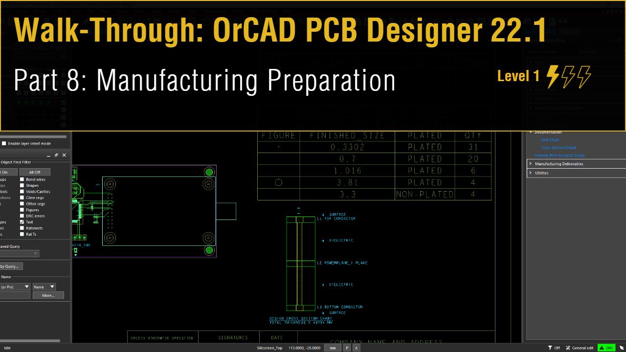
Lesson 8: Manufacturing Preparation
This walk-through demonstrates how to prepare your board for manufacturing and generate manufacturing data in OrCAD PCB Designer 22.1 (2022). After you complete this topic, you will be able to:
- Add dimensions and title block for fabrication
- Create a Drill Chart and Cross Section Chart
- Setup Artwork Films
To follow along, continue with the design from the previous lesson or use the downloaded materials.
If materials were not downloaded at the start of the walk-through, they can be accessed in the Materials tab of this lesson.
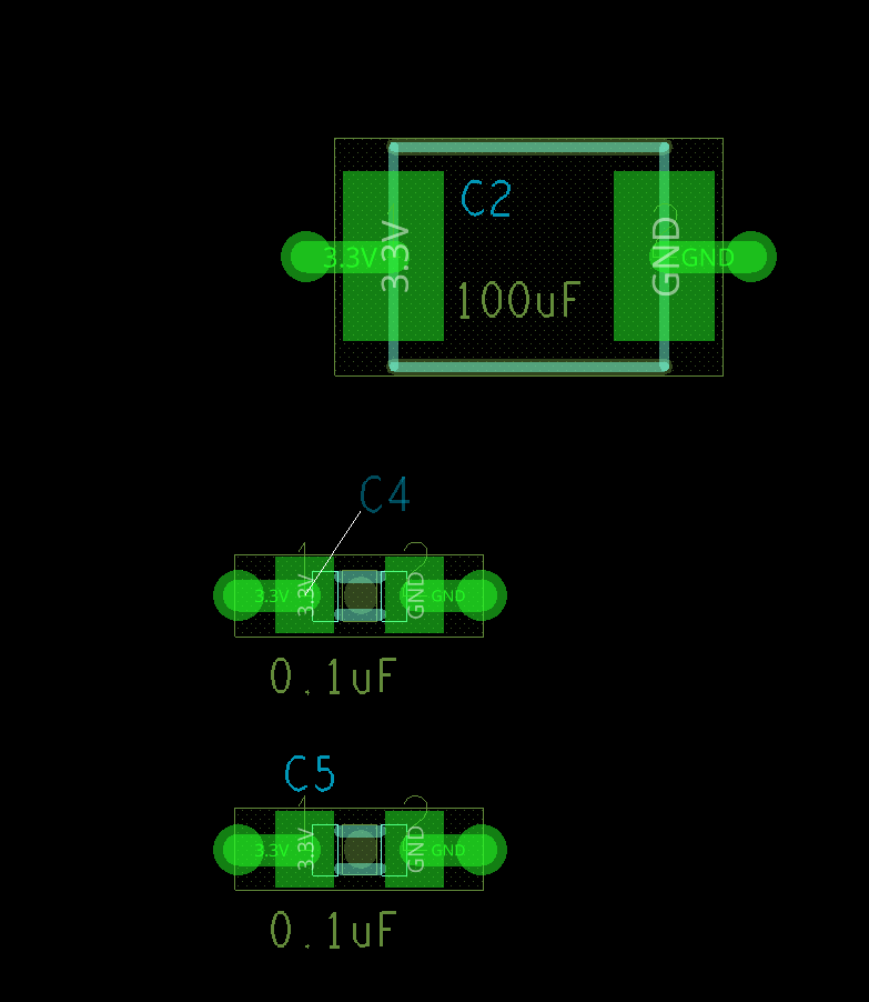
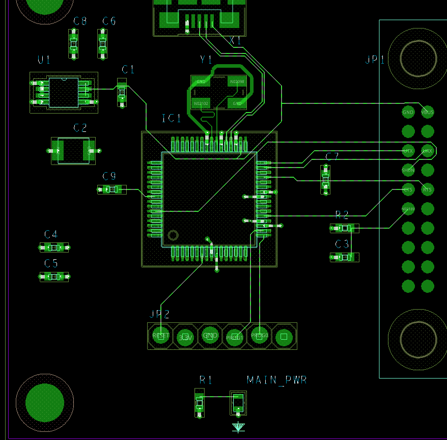
 Open in New Window
Adjusting Visibility
Step 1: Select Setup > Colors from the menu or the Color192 button on the toolbar.
Step 2: Select the Nets tab.
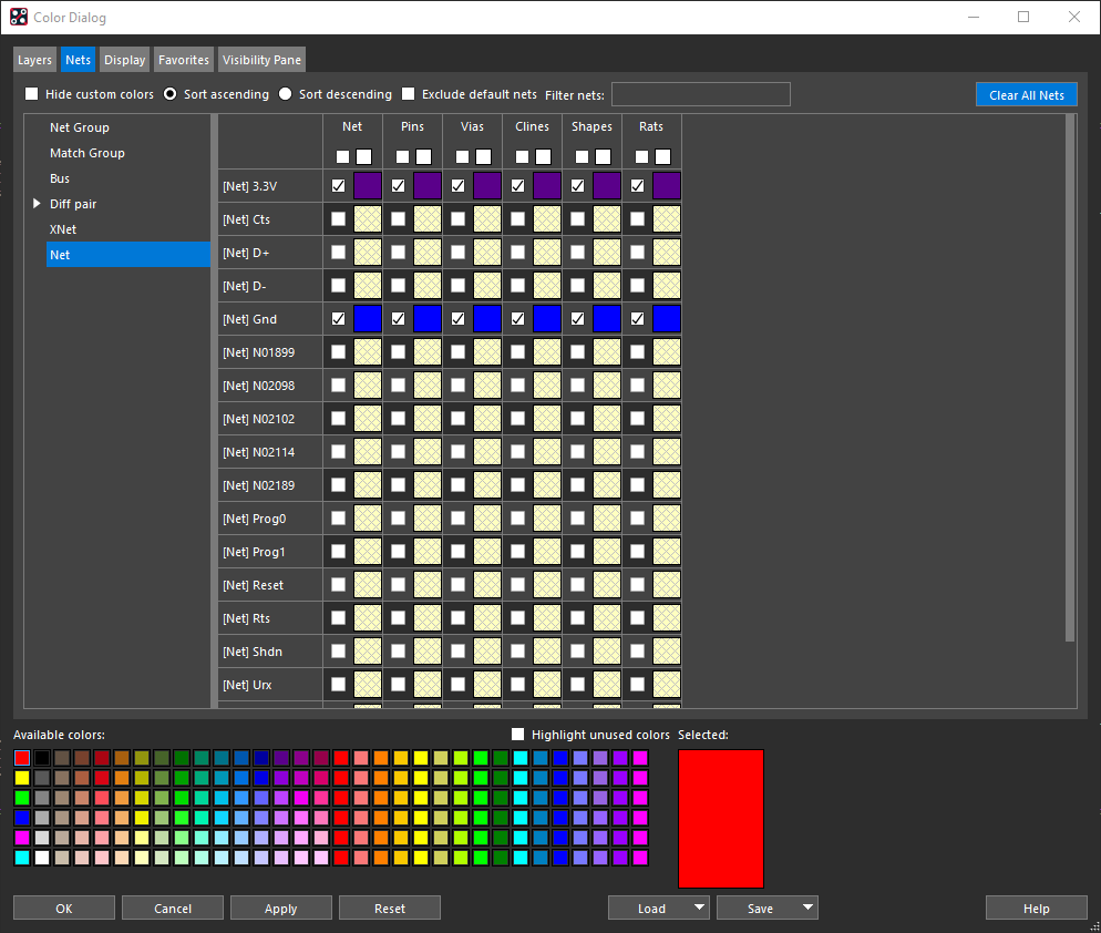
Step 3: Select Clear All Nets.
Note: This will clear the net color overrides defined in a previous lesson.
Step 4: You will be prompted to clear the nets. Click Yes.
Step 5: Click OK to apply the changes and close the window.
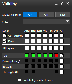
Step 6: Select On for Global Visibility in the Visibility panel.
Step 7: Select All On in the Find panel.
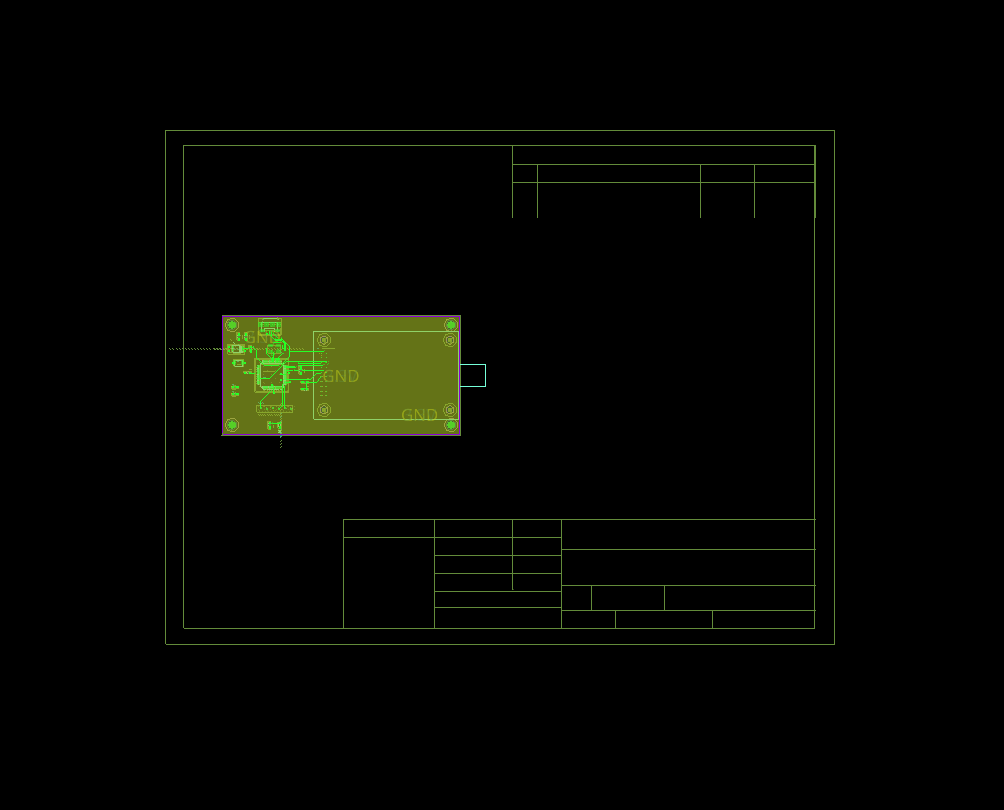
Placing the Outline
Step 8: Select Place > Components Manually from the menu.
Step 9: Select the Advanced Settings tab.
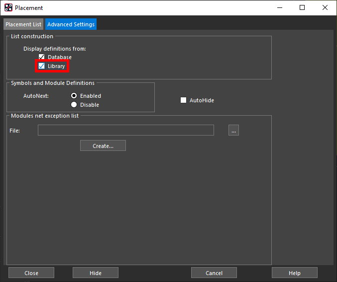
Step 10: Under List Construction and Display Definitions From, check Library.
Step 11: Select the Placement List tab.
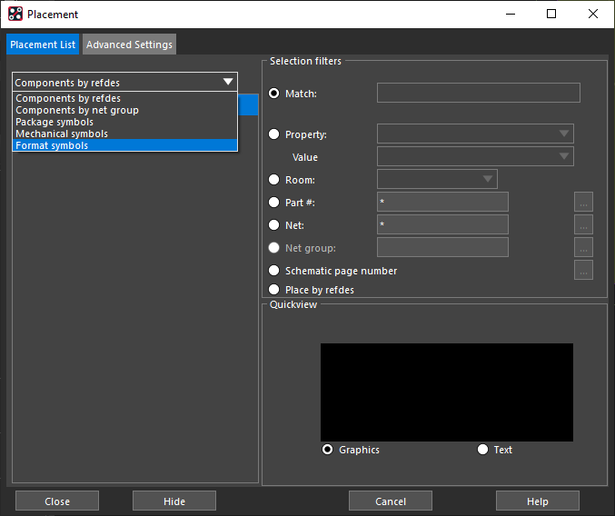
Step 12: Select Format Symbols from the drop-down menu above the list.
Step 13: Check the box next to ASIZEH to place the outline.
Step 14: Click the canvas to place the outline.
Step 15: Click Close in the placement window to save the placement and close the window.
Note: If you close with the ‘x’ button in the header bar, the outline will not be placed. If the outline does not fit, use the following steps to re-center the board and adjust the origin.
- Unfix the crystal traces before moving the board. Select the traces, right-click, and select Unfix.
- Click and drag to highlight the whole board.
- Select the Move button from the toolbar.
- Click the board to move it. Zoom out to view the full PCB canvas, then click again to place the board in the center of the canvas.
- Zoom into the bottom-left corner of the board.
- Select Setup > Change Origin from the menu.
- Right-click the corner and select Snap Pick To > Segment Vertex. The origin snaps to the corner.
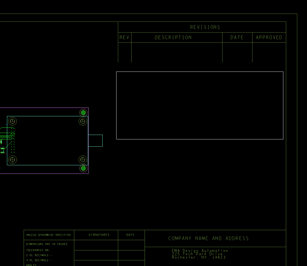
Adding Title Block Information
Step 16: Select Add > Text from the menu.
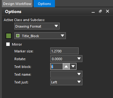
Step 17: In the Options panel, select Drawing Format from the Active Class dropdown and Title_Block from the Active Subclass dropdown.
Step 18: Set the Text Block to 6.
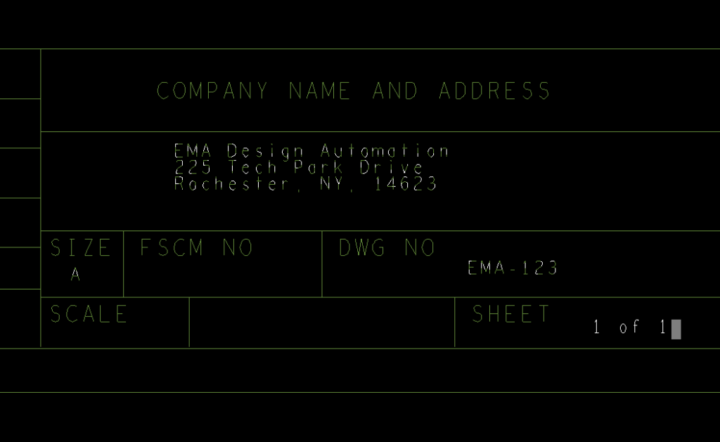
Step 19: Fill the title block with your company’s required information. Click to start writing a line of text. When finished with that line, click again to write elsewhere. When finished, right-click and select Done.
Adjusting Text
Step 20: Select Last under Global Visibility in the Visibility panel.
Note: This will change the visibility settings to their last configuration.
Step 21: In the Find panel, select All Off, then check Text.
Step 22: Click and drag to move component text around as needed. To delete, select the text, right-click, and select Delete. To rotate, select the text, right-click, and select Spin.
Step 23: Select Edit > Change Objects from the menu.
Step 24: Uncheck Line Width and check Text Block.
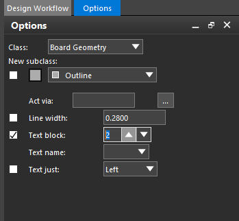
Step 25: Set the Text Block value to 2.
Step 26: Click the reference designator text for each component or highlight the design to select all reference designators. Right-click and select Done.
Note: All reference designators are changed to text block size 2.
Placing Drill and Cross Section Information
Step 27: Select Manufacture > Customize Drill Table from the menu.
Step 28: Select Validate.
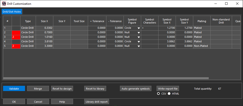
Note: Some of the cells will be highlighted in red, indicating that two of these holes have identical definitions. For this board, this is fine.
Step 29: Select Auto Generate Symbols. Click Yes when prompted.
Step 30: Click OK.
Step 31: In the Design Workflow, select Manufacturing Preparation > Documentation > Drill Chart.
Step 32: Leave the default settings and click OK to create the drill chart.
Step 33: Click the canvas to place the drill chart.
Step 34: Select Manufacturing Preparation > Documentation > Cross Section Detail from the Design Workflow.
Step 35: In the Cross Section Chart window, set the Text Block to 3.
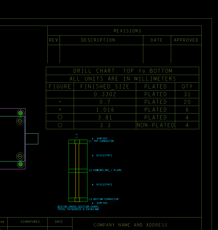
Step 36: Click OK and click to place in the canvas.
Adding Dimensions
Step 37: Select Manufacture > Dimension Environment from the menu.
Step 38: Right-click and select Linear Dimension.
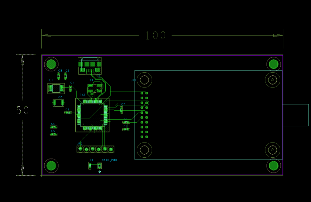
Step 39: Click the corners of the board to dimension and click to place the dimension. When finished, right-click and select Done.
Configuring the Artwork Path
Step 40: Select Setup > User Preferences from the menu.
Step 41: In the Category list, expand File_management and select Output_dir.
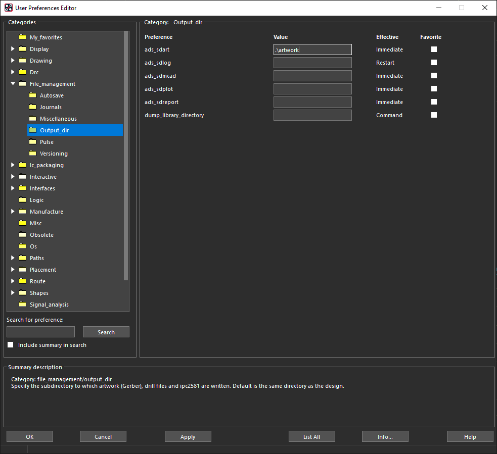
Step 42: Enter the text .\artwork into the first field, ADS_sdart. Click OK.
Note: This will create a folder for your exported artwork.
Creating Artwork Film
Step 43: Select Setup > Colors from the menu or the Color192 icon from the toolbar.
Step 44: Select the Layers tab.
Step 45: Select Off for Global Visibility.
Note: This will turn off all layers and ensure only the necessary layers are selected.
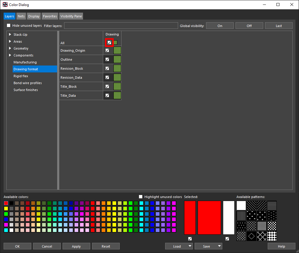
Step 46: Select Drawing Format from the list on the left and check the box for All to enable visibility for all Drawing Format components.
Step 47: Select Manufacturing and check the boxes for NClegend1-3 and Xsection_Chart.
Step 48: Select Geometry and check the boxes for Design_Outline and Dimension.
Step 49: Click Apply.
Step 50: Select Manufacturing Preparation > Artwork (Film Records) Setup from the Design Workflow.
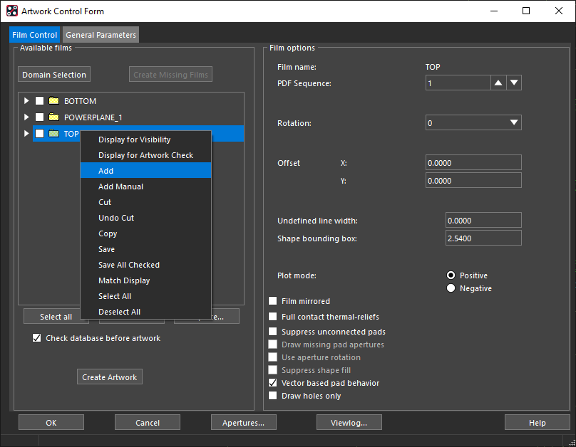
Step 51: Right-click one of the entries in the film window and select Add.
Step 52: Name the film FAB and click OK.
Step 53: Select the new film and change the Undefined Line Width to 0.127.
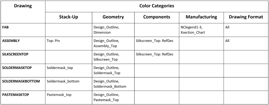
Step 54: Repeat steps 52-59 for all Artwork Films using the table below:
Step 55: Close the Color Dialog window.
Step 56: Click OK to close the Artwork Control Form.