PCB Footprints and 3D Models
This lesson will demonstrate how to replace pins in a PCB footprint, map 3D models to components, and add 3D models to the design for mechanical enclosures and connectors.
To follow along, continue with the design from the previous lesson or download the starting materials from the Materials tab of this lesson.
 Open in New Window
Activating the Footprint Editor
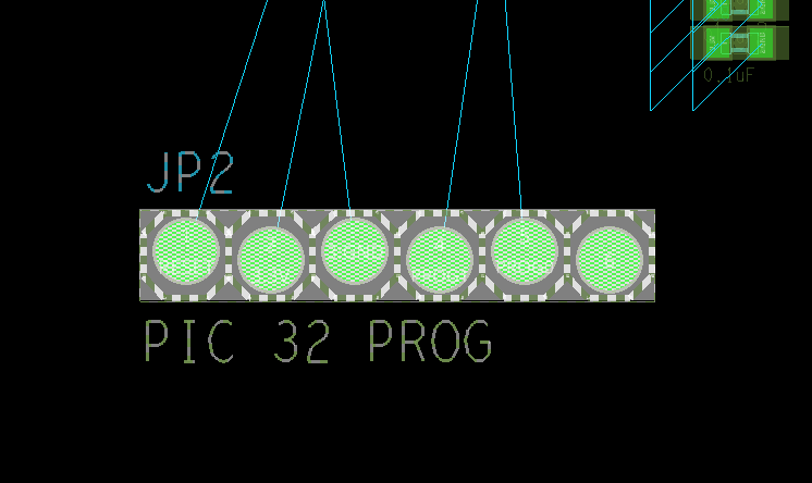
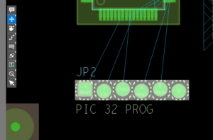
Step 1: Select the 1×6 header, JP2, in the PCB canvas.
Step 2: Right-click the header and select Edit Footprint. The Footprint Editor opens in a similar window to Presto, with the header footprint in the center.
Replacing a Padstack

Step 3: Select the leftmost pad which corresponds to pin #1.
Step 4: Right-click the pad and select Replace Padstack.
Step 5: The Replace Padstack widget opens. Select Update Selected.
Note: This will update only the selected pin. To modify all the padstacks used in the component select Update All.
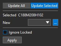
Step 6: Select the ellipsis to add a new padstack.
Step 7: Browse to the provided pad65sq37d.pad file, select it, and click Open.

Step 8: Click Apply. The pin is now square and the remaining pins are still circular.
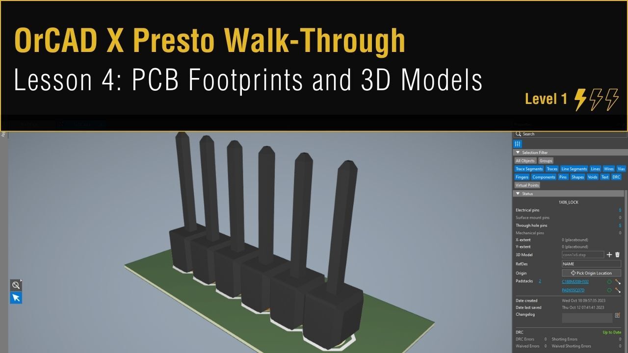
Assigning a 3D Model
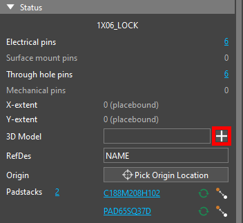
Step 9: In the Properties panel, select the plus sign for 3D Model to assign a 3D model.
Step 10: Browse to the location of the provided conn1x6.step model. Select the file and click Open.
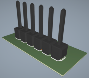
Step 11: View the assigned 3D model. The footprint is now associated with a 1×6 header model.
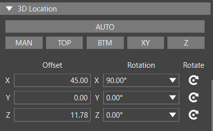
Note: If the 3D model is not automatically mapped correctly, there are multiple methods to adjust the model mapping including:
- AUTO: Attempt to automatically align the 3D model with the footprint using the existing placebound geometry.
- MAN: Manually drag the 3D model into the correct location.
- TOP: Snap a single face from the 3D model to the top of the PCB surface.
- BTM: Snap a single face from the 3D model to the bottom of the PCB surface.
- XY: Align a number of elements from both the 3D model and the footprint or PCB in the XY plane.
- Z: Align one or more faces from the 3D model and the footprint or PCB in the Z direction.
- X, Y, and Z Offset and Rotation: Manually enter values for the offset and rotation in the X, Y, and/or Z directions.
Step 12: Select the Visibility button on the left side of the screen to open the Visibility panel.
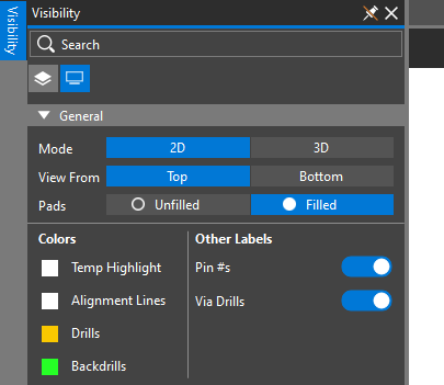
Step 13: Select 2D for the Mode under General to return to the 2D mode.
Updating the Footprint
Step 14: Select File > Save 1x06_lock.dra from the menu.
Step 15: A prompt will appear to overwrite the file. Click Yes.
Step 16: Close Footprint Editor.
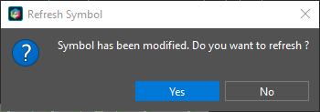
Step 17: A prompt will appear that the symbol has been modified. Click Yes to refresh.
Note: If your system has multiple monitors, this prompt may appear behind another window.
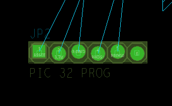
Step 18: View the canvas. JP2 now has a square pad on the leftmost pin.
Note: If the component does not update automatically, perform the following steps to update it.
- Step 1: Select the component and press Delete on the keyboard.
- Step 2: Select ECO > Quickplace Components from the menu. Only the unplaced components are placed, in this case, only JP2.
- Step 3: Select the Move mode from the toolbar.
- Step 4: Click to place the updated JP2 in its original location. Press Escape on the keyboard or select the Select mode from the toolbar when finished.
Mapping the USB Connector
Step 19: Select Visibility to open the Visibility panel.
Step 20: In the Display mode, select 3D to open the 3D viewer. The 3D viewer window opens, showing the board with placement guides to highlight component locations.
Step 21: Select the Component mode in the Visibility panel.
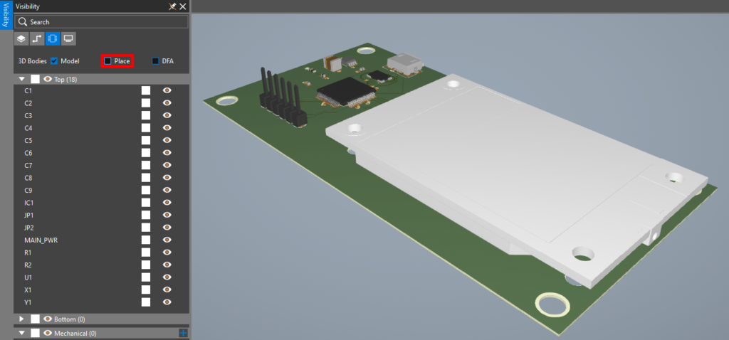
Step 22: Under 3D Bodies, uncheck Place. The 3D placement boundaries are removed. This will improve visibility when analyzing collisions visually.
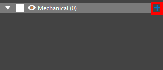
Step 23: Expand Mechanical and select the plus sign to add a new mechanical model.
Step 24: Browse to the provided 3D models and select USB.STEP. The mechanical model is added as USB.
Step 25: Select the USB connector in the canvas.
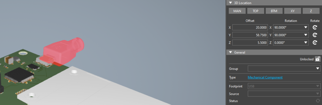
Step 26: In the Properties panel, under 3D Location, enter the following parameters:
- X Offset: 20
- Y Offset: 58.75
- Z Offset: 5.5
- X Rotation: 90
- Y Rotation: 90
Step 27: Pan the view as needed to view the connector. The connector lines up with the USB port.
Mapping the Enclosure
Step 28: Select Visibility to open the Visibility panel.
Step 29: Select the Component mode if it is not already selected.
Step 30: Select the plus sign next to Mechanical. Browse to the location of the provided 3D models and select Enclosure.STEP.
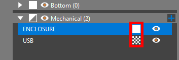
Note: Mechanical symbols are imported as transparent by default. Select the checker pattern to make the model opaque.
Step 31: Select the enclosure to open its properties.
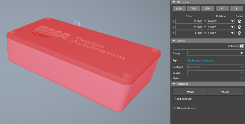
Step 32: In the Properties panel, under 3D Location, enter the following parameters:
- X Offset: 50.5
- Y Offset: 25
- Z Offset: 4
- X Rotation: 90
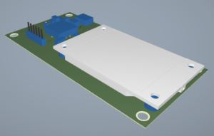
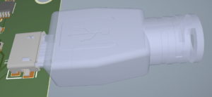
Step 33: View the mapped enclosure.
Step 34: In the Visibility panel, in the Display mode, select 2D to return to 2D mode.