PCB Walk-through 10: 3D Modeling
This walk-through demonstrates complete STEP Model mapping and collision detection. After you complete this topic, you will be able to:
- Map 3D Models to PCB footprints
- Add mechanical housing and models
- Perform collision detection
- Cross-probe between 2D and 3D to resolve collisions
To follow along, continue working with the design completed in PCB Walkthrough 9 or open the provided board file in the folder directory, PCB Walkthrough 10_3D Modeling.
If design files were not downloaded in the beginning of the walk-through, they can be accessed through the Materials tab above.
 Open in New Window
Note: To change the view to replicate what is shown in the video, select the Color button from the toolbar. Change the colors to the following:
- Stack-up: Select All except Powerplane_1 and Bottom
- Area: Select All
- Geometry: Select All except Dimension
- Components: Select All
- Manufacturing: Remove All
- Drawing Format: Remove All
Click OK to close the Color Window.
- Select the Move button from the toolbar and select the USB Connector, X1.
- In the Command Window, type x 20 46 and Enter.
Note: This move is required for proper integration with the mechanical enclosure. If any changes are made to the board, manufacturing artwork and documentation will require regeneration.
- Select Y1 and click to place on the PCB Canvas to ensure there is no interference with the USB Connector, X1.
- Select the Delete button on the toolbar and select traces that have been unconnected due moving the components.
- Select Route > Connect from the menu and route the unconnected traces. Right click and select Done.
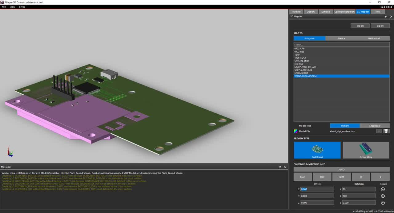
- Select the 3D button from the toolbar or Display > 3D Canvas from the menu.
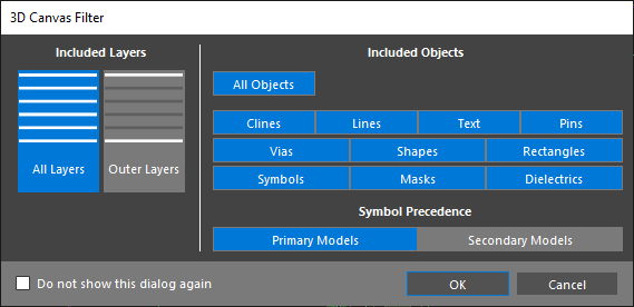
Note: When first selecting the 3D Canvas, the 3D Canvas Filter will be activated. Here you can select which portions of the design are included in the 3D representation. Within the 3D canvas, you can select which layers are visible in the visibility tab. You can select which models are visible in the symbols tab. By default, any components without 3D models are represented with a boundary shape. To change this, select Setup > Preferences > Symbol Representation and select the desired display for each symbol.
- In the 3D canvas, select the 3D Mapper tab.
Note: If this window is not activated, select View > Windows > 3D Mapper.
- In the Map To Window, select Footprint and choose 1210 from the list of components.
- Select Primary as the Model Type.
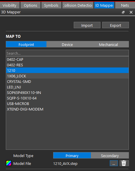
- Browse for the model file and select 1210_AVX.step.
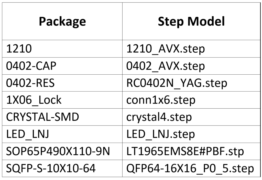
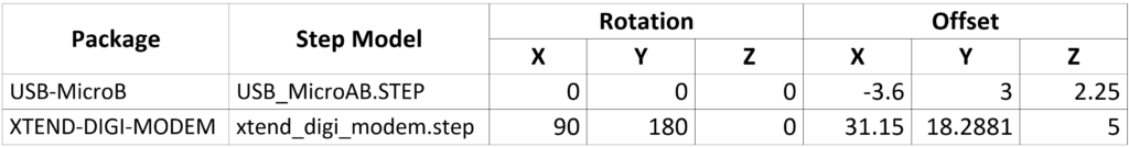
- Complete the STEP Mapping for all the components using the table below:
Note: No adjustments need to be made for these step models as they are automatically aligned to the PCB footprints.
- Complete the STEP Mapping for the following components by adjusting the rotation and offset according to the table below:
Note: The 3D Mapper includes several options for quick and efficient model mapping including automatic mapping, manual mapping, mapping to the top or bottom of the board, and more.
- Under Map To, select Mechanical. Double-click Create Mechanical Model.
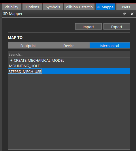
- Double-click the newly created model to change the name. Enter the name STEP3D_MECH_USB and Enter or click outside the text box.
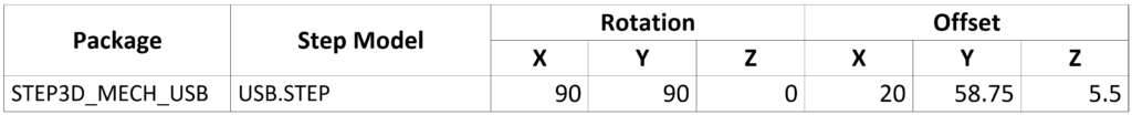
- Map USB.STEP to the new mechanical package using the table below:
Note: Select View > Camera from the menu to change the view and ensure the STEP file is mapped correctly. To rotate the board in the 3D Canvas, hold down the SHIFT key on the keyboard and press the middle mouse button.
- Double-click Create Mechanical Model.
- Enter the name STEP3D_MECH_ENCLOSURE and Enter or click outside the text box.
- Map Enclosure.STEP to the new mechanical package using the table below:

Note: To turn visibility on/off for mechanical symbols and components in the design select View > Windows > Symbols from the menu. To adjust the transparency of the mechanical models, select Setup > Preferences > Symbol Representation from the menu.
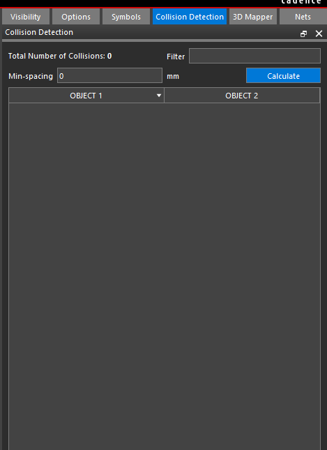
- Select the Collision Detection tab and select Calculate.
Note: If this tab is not visible, select View > Windows > Collision Detection from the menu.
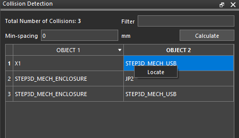
- Right click on an item and select Locate or select an item from the list to highlight the component in the 3D view.
Note: The Locate command will make the component flash for easy detection. Enable the cutting plane to view a cross section of the PCB to help determine collision and design structure issues. Right click the 3D Canvas and select Cutting Plane. Check Enable Cutting Plane. Adjust the Offset and Tilt in the X, Y, and Z directions for more detail. Right click and select Done when finished.
- Select Setup > Preferences from the menu.
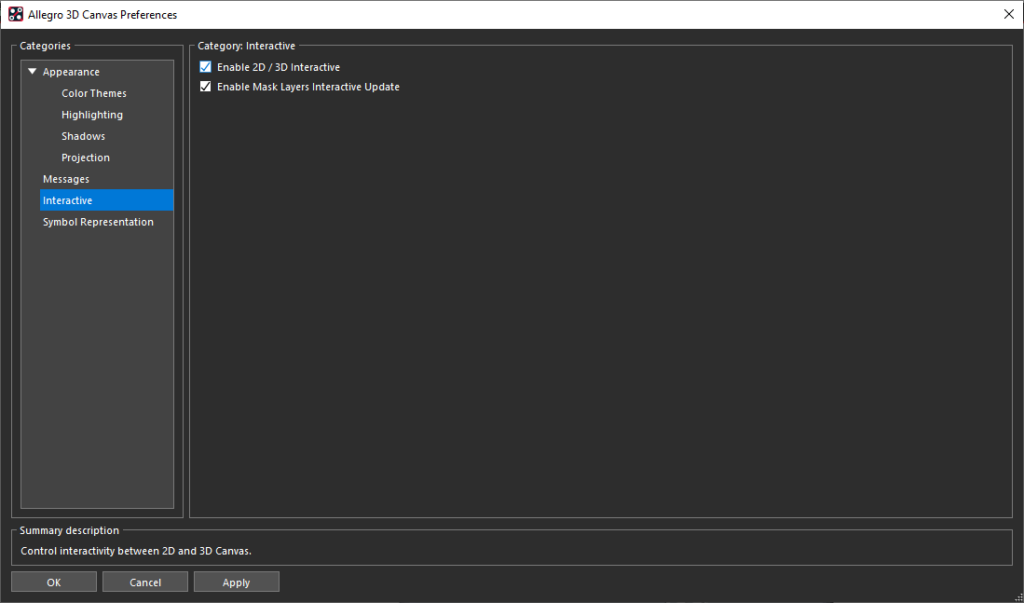
- Select Interactive and check Enable 2D/3D Interactive. Click OK.
Note: To rotate the board hold down the shift key and middle mouse button or you can choose preset views by selecting View > Camera in the menu.
- Set up a split screen between the PCB Canvas and the 3D Canvas.
- Click to move the connector JP2 in the PCB to line up with the existing cutout on the enclosure.
Note: The changes will appear automatically in the 3D view once the part is placed.
- Re-route the connections.
Note: Delete the existing traces. In the Design Window, select Interconnect > Manual Routing > Add Connect. Click to place the trace. Right click and select Done when finished. In the Design Workflow, select Display Status to confirm the routing.
- In the Collision Detection tab, select Calculate.
Note: The errors have been resolved and only the collision between X1 and the USB is reported.
- Back in the PCB Canvas, select File > Save (CTRL-S) from the menu or the Save button on the toolbar. Select YES to overwrite the design.
- In the 3D Canvas, select File > Export.
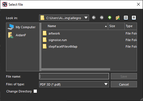
- Select PDF 3D as the file type.
- Name the file and click OK.
