PCB Walk-through 4: Constraints
This walk-through demonstrates how to set up differential pairs and constraints using OrCAD PCB Designer Professional. After you complete this topic, you will be able to:
- Set up a differential pair
- Specify electrical, physical and differential pair rules with Constraint Sets
- Use Design Sync to communicate the required constraints
To follow along, continue working with the design completed in PCB Walkthrough 3 or open the provided board file in the folder directory, PCB Walkthrough 4_Constraints.
If design files were not downloaded in the beginning of the walk-through, they can be accessed in the Materials tab above.
 Open in New Window
- Open the schematic in OrCAD Capture.
- Select PCB > Update Layout from the menu. Select Sync.
- Select the desired version of OrCAD PCB Designer from the software selection window.
Note: This will enable a constraint driven design flow and sync the designs. If If you did not define your differential pairs at the schematic level, use the following steps for definition in the PCB:
- Select Setup > Add Differential Pairs from the menu.
- Select Auto Generate.
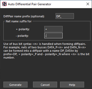
- Assign DP_ for the name.
- Set the + polarity to +.
- Set the – polarity to –.
- Click Generate.
- Click OK to close the window.
This has generated the differential pair.
- In OrCAD PCB Designer, select Constraints > Modes. from the Design Workflow
Note: In the Modes window, select which constraints will be checked by setting the constraints “On” or “Off”. Electrical constraints are available in OrCAD PCB Designer Professional.
- Close the Mode window.
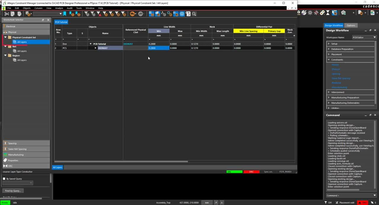
- In the Design Workflow, select Constraints > Physical.
Note: This opens the constraint manager window. In the constraint manager, you can assign electrical, physical, and spacing constraints. Assign constraints by creating Csets or assigning values to each individual net.
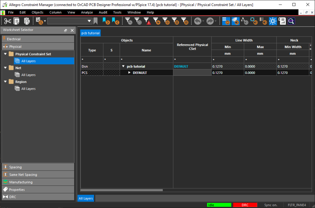
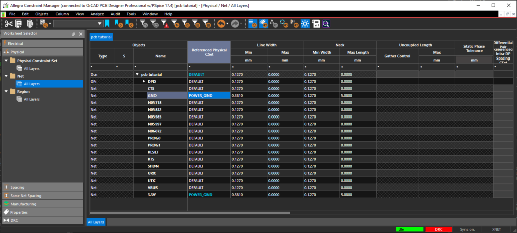
- In the constraint manager window, select the Physical Constraint Set > All Layers.
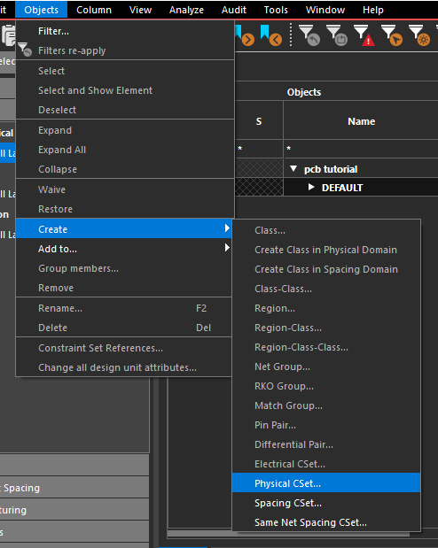
- Right click and select Create > Physical CSet.
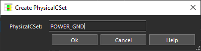
- Name the constraint set POWER_GND and click OK.
- Set the following constraint values:
- Minimum line width: 0.381
- Minimum neck width: 0.127
- Maximum neck length: 5.08
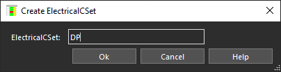
- Right click and select Create> Physical CSet.
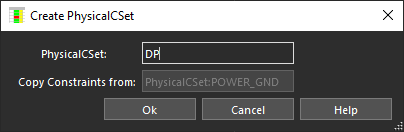
- Name the constraint set DP and click OK.
- Set the following constraint values:
- Line Width: 0.127
- Primary Gap: 0.127
- In the worksheet selector, select Net > All Layers.
- In the Referenced Physical CSet column, assign the POWER_GND CSet to 3.3V and GND.
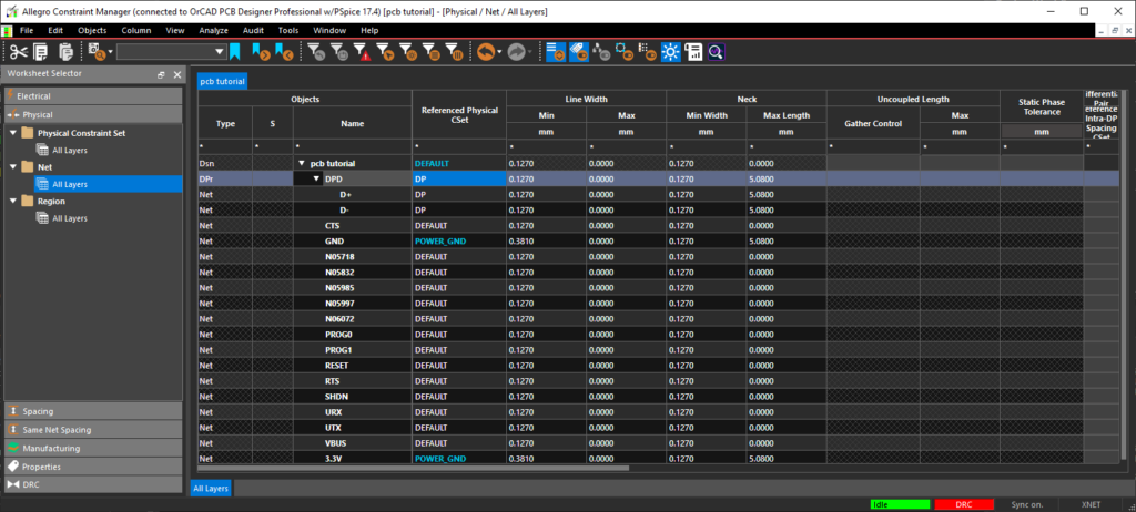
- In the Referenced Physical CSet column, assign the DP CSet to DPD.
Note: Assign the differential pair Cset (DP) at the top level to apply to each net.
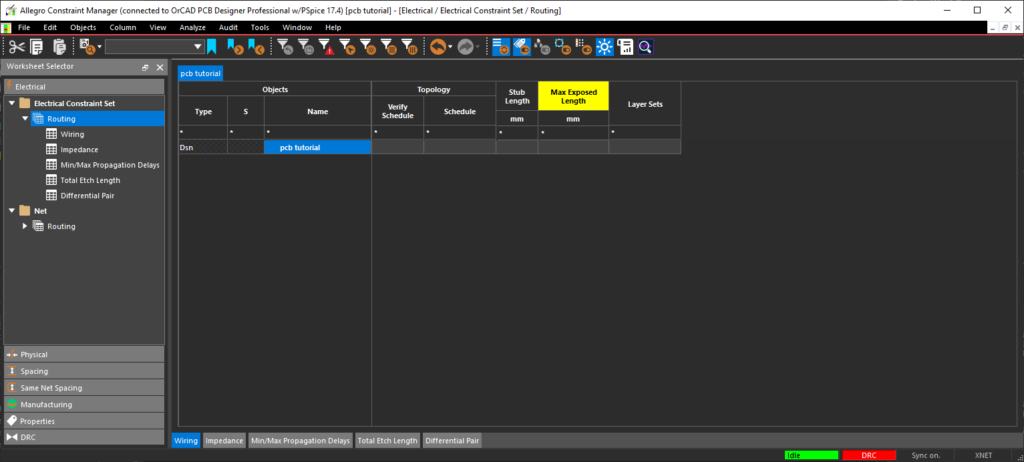
- In the worksheet selector, select Electrical > Electrical Constraint Set > Routing.
- Right click and select Create > Electrical CSet.
- Name the CSet DP and click OK.
- In the worksheet selector, select Electrical Constraint Set > Routing > Differential Pair. Set the following constraint values:
- Gather Control: Ignore
- Uncoupled Length: 5.08
- Static Phase Tolerance: 0.508
- In the Worksheet Selector, select Net > Routing > Differential Pair.
- In the Referenced Electrical CSet column, assign the DP Cset to DPD.
- In the Worksheet Selector, select Properties > Net > General Properties.
- Assign 0 to GND.
- Assign 3.3 to 3.3V.
- Close the Constraint Manager Window.
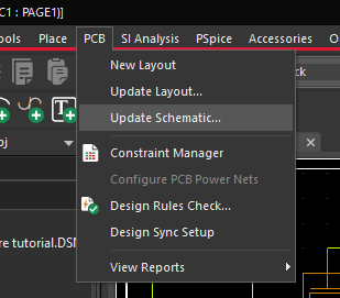
- Back in OrCAD Capture, select PCB > Update Schematic.
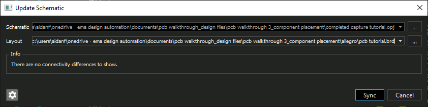
- Select Sync.
Note: This will synchronize the schematic and PCB, bringing in any changes made in the PCB Design into the schematic. The same process can be completed to push changes from the schematic to the layout by selecting PCB > Update Layout from the menu.
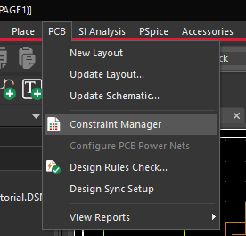
- In OrCAD Capture, select the constraint manager button on the toolbar or PCB > Constraint Manager from the menu.
- Click OK.
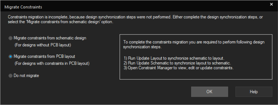
Note: If you see a window titled Migrate Constraints after clicking OK, the layout and schematic were not updated.
- Select Migrate constraints from PCB layout.
- Click OK.
- Select PCB > Update Layout.
- Click Sync.
- Select PCB > Update Schematic.
- Click Sync.
- Select PCB > Constraint Manager and try again.
- The constraints assigned in OrCAD PCB Designer are now visible in OrCAD Capture. These rules are embedded in the design database and for easy communication between the physical and logical designs.