Performing a Design Rule Check
This lesson will demonstrate how to perform design rule checks and correct errors in OrCAD X Presto.
To follow along, continue with the design from the previous lesson or download the starting materials from the Materials tab of this lesson.
 Open in New Window
Activating DRC Checks
Note: DRC checks must be activated before any errors are reported.
Step 1: Select Tools > Constraint Manager from the menu.
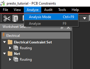
Step 2: Select Analyze > Analysis Mode from the Constraint Manager menu. The Analysis Modes window opens.
Step 3: Select Physical from the list on the left. From here, constraint checks can be enabled or disabled. Select the checkbox in the On column to activate a constraint check and Off to disable the constraint check.
Step 4: Select the On checkbox for Mark All Constraints to activate all constraint checks.
Step 5: Select Electrical. Click the On checkbox for Mark All Constraints to activate all constraint checks.
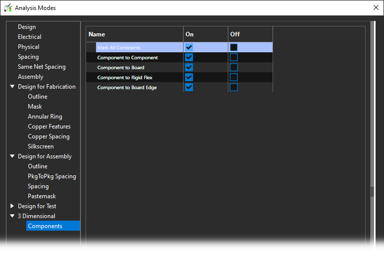
Step 6: Select 3 Dimensional > Components. Click the On checkbox for Mark All Constraints to activate all constraint checks.
Step 7: Click OK to save the settings and close the window. Close the Constraint Manager.
Checking for DRC Errors
Step 8: In the Properties panel, select the Refresh button for DRC to refresh the DRC cache.
Note: If a Refresh button for Out of Date Shapes is visible above, refresh the shapes then refresh the DRC.
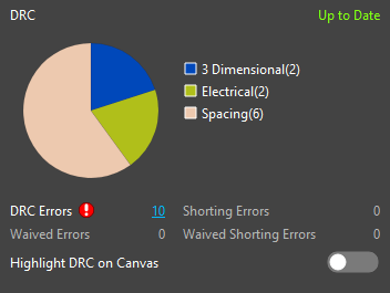
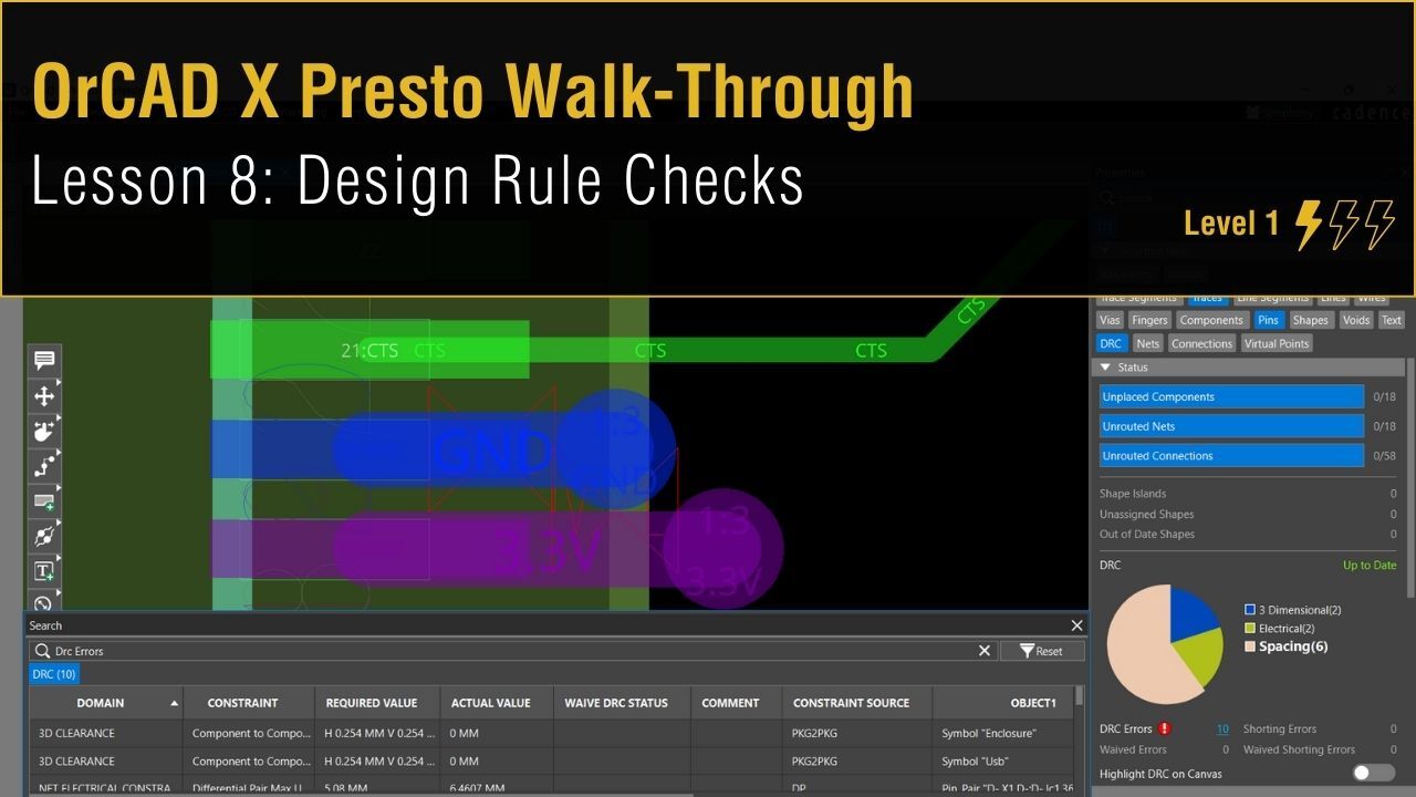
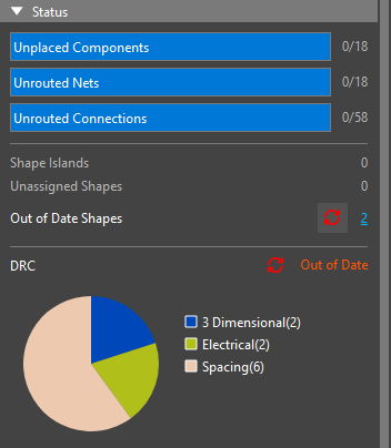
Step 9: View the DRC subpanel. A pie chart is used to distinguish the type of errors. There are six spacing errors, two electrical errors, and two 3D errors.
Note: There may be additional errors depending on how the specific design was completed.
Step 10: Click the Spacing portion of the pie chart to open a list of the spacing design rule errors in the Search panel.
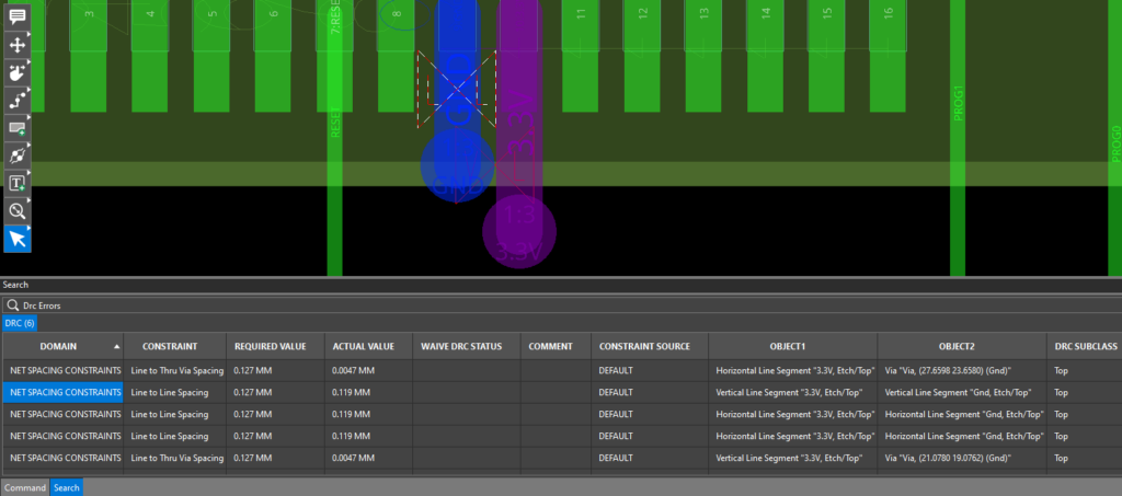
Step 11: Double-click the first spacing constraint to be brought to the location of the marker. The required line-to-line spacing is specified as 0.127mm, while these lines are 0.119mm apart.
Correcting Spacing DRCs
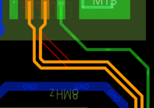
Step 12: In the Selection Filter subpanel of the Properties window, disable All Objects and click Pins to enable the selection of pins.
Step 13: Right-click the Add Connect icon from the toolbar. Select the Fanout icon.
Step 14: In the Fanout widget, change the trace width to 0.280, the mode to Linear and the direction to IN.
Step 15: Click to select each of the GND traces for the IC that have DRC errors. The fanout traces are redrawn going inward with a thinner trace.
Step 16: When finished, press Escape on the keyboard or select the Select mode from the toolbar.
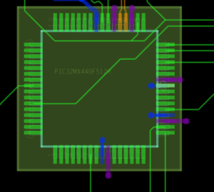
Step 17: Click anywhere in the canvas to deselect any objects that are still selected. View the DRC subpanel in the Properties panel. Only the 3D and electrical constraint violations remain.
Correcting Electrical DRCs
Note: The presence/severity of these DRC errors depends on how the differential pair DPD was routed in the previous lesson.
Step 18: Click the Electrical section of the DRC pie chart to open the list of Electrical design rule errors in the Search panel. The listed electrical constraint violations show that both differential pair traces violate the maximum uncoupled length.
Step 19: Select the Slide mode from the toolbar.
Note: Diagonal line segments are considered uncoupled due to the extra distance between the traces.
Step 20: Click to select one of the trace segments. The corresponding segment on the other net is automatically selected as well. Reduce the length of the diagonal segment and click again to place the traces.
Step 21: Press Escape on the keyboard or select the Select mode from the toolbar.
Step 22: View the Properties panel. Only the two 3D errors remain.
Correcting 3D Clearance Errors
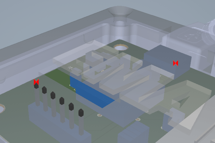
Step 23: Click the hyperlinked number of DRCs to open the list in the Search panel. Two 3D constraint violations are listed. One is between the mechanical USB connector and X1, the other is between the enclosure and JP2.
Step 24: Open the Visibility panel and select the Display mode. Select 3D to activate the 3D view. The DRC markers are visible in the 3D canvas.
Step 25: Enable Components in the Selection Filter subpanel.
Step 26: Select JP2 on the board.
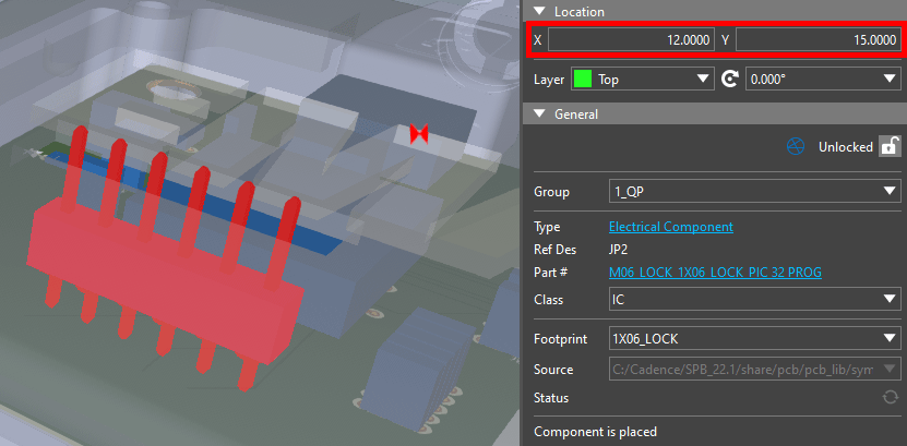
Step 27: In the Properties panel, under Location, enter 12 for X and 15 for Y. The connector is moved to clear the opening in the enclosure.
Note: Traces will need to be rerouted after moving the connector.
Step 28: Open the Visibility panel and select the Display mode. Select 2D to return to the 2D mode.
Step 29: Disable Trace Segments in the Selection Filter and enable Traces.
Step 30: Click and drag to select the three traces that originally went to JP2. Press Delete on the keyboard.
Step 31: Right-click the Fanout mode and select the Add Connect mode from the toolbar.
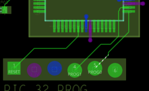
Step 32: Click to route new traces on the RESET, PROG0, and PROG1 nets. Press Escape or select the Select mode when finished.
Step 33: View the DRC section of the Properties panel. Only one 3D error remains.
Waiving DRCs
Step 34: Click the hyperlinked number of DRCs to open the list in the Search panel. The last DRC violation is between the mechanical USB connector and X1. Since these components are supposed to connect in the final design, a collision is expected and this error can be ignored.
Step 35: Double-click the error to select the marker and pan to its location.
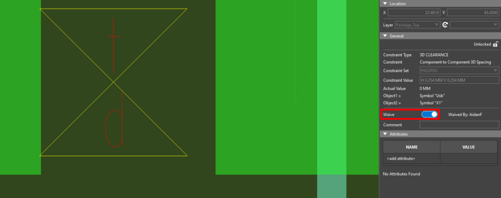
Step 36: In the Properties panel, under General, enable the Waive option to waive the error.
Note: The marker is now vertical. The Properties panel now lists the name of the user who waived the error.
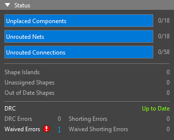
Step 37: Click anywhere to deselect the marker. The DRC error count is now 0, and the Waived Error count is 1.
