PCB Walk-through 6: Routing
This walk-through demonstrates how to route your PCB. After you complete this topic, you will be able to:
- Route and clean-up traces
- Verify all nets are routed
To follow along, continue working with the design completed in PCB Walkthrough 5 or open the provided board file in the folder directory, PCB Walkthrough 6_Routing.
If design files were not downloaded in the beginning of the walk-through, they can be accessed through the Materials tab above.
 Open in New Window
- Select the Color button from the toolbar.
- In the Layers tab, click the All check box twice.
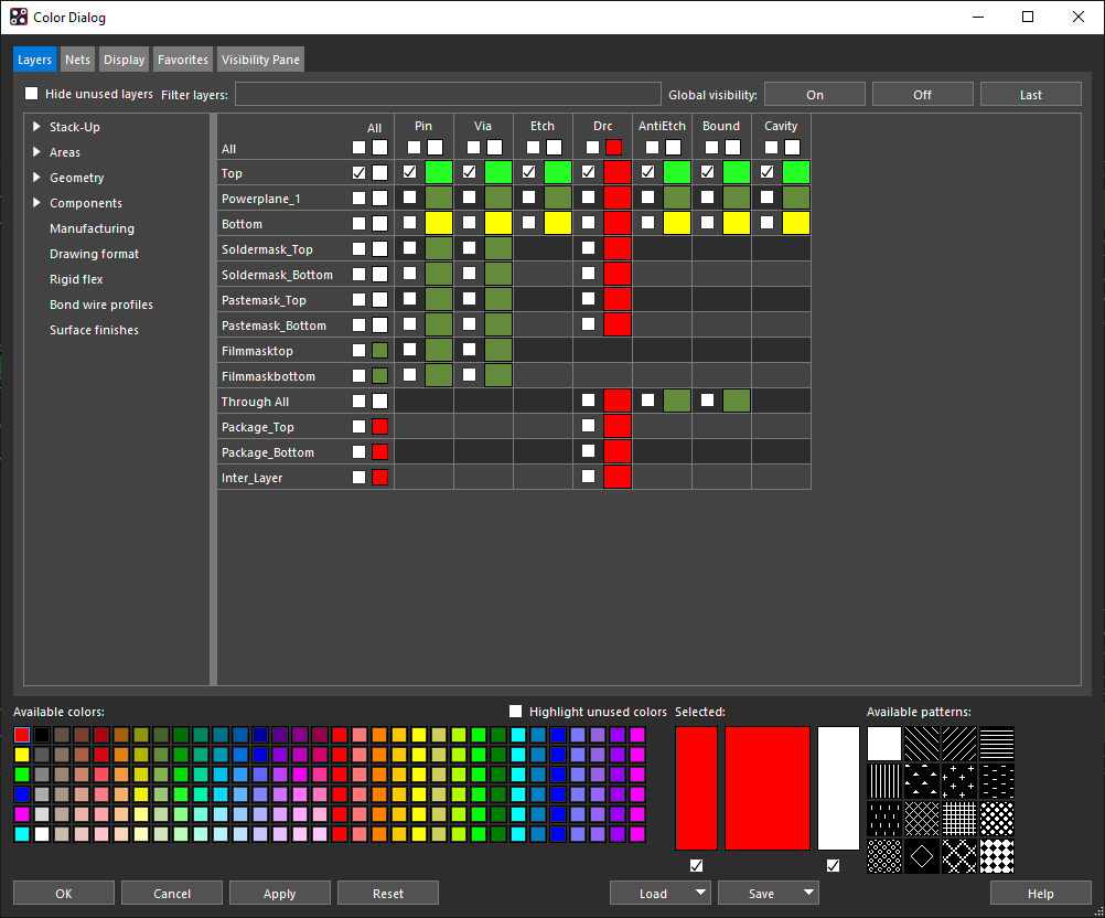
- Select the All check box for Top.
- Select the Net tab.
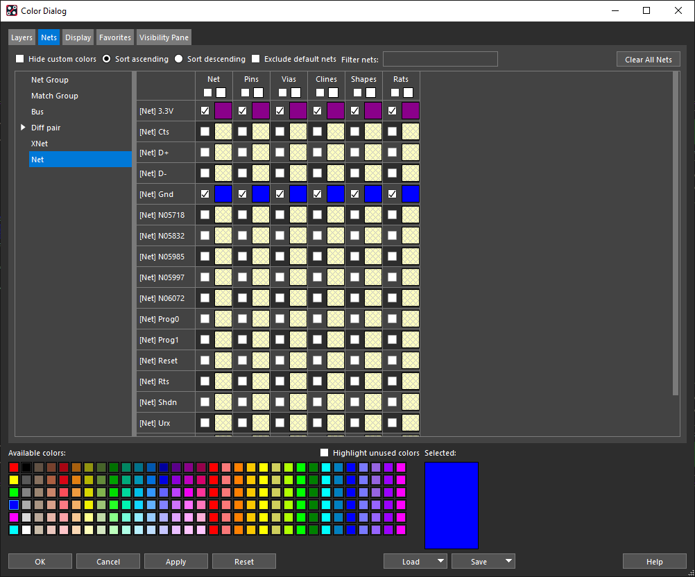
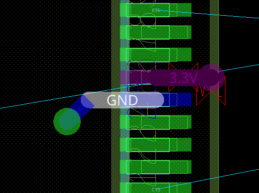
- Select purple from the Available Colors then select Net 3.3V.
- Select blue from the Available Colors then select Net GND.
- Click OK.
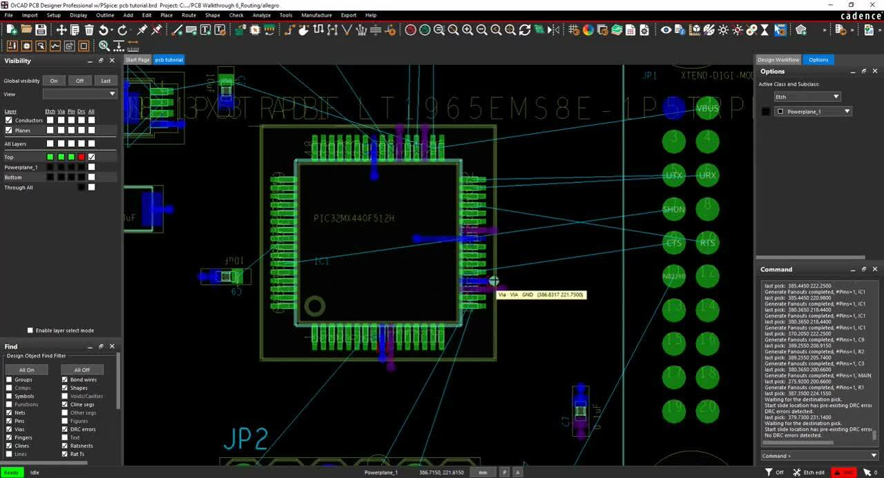
- Select Route > Create Fanout from the menu.
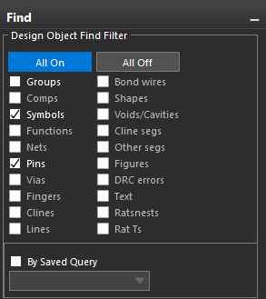
- In the Find tab, select All On.
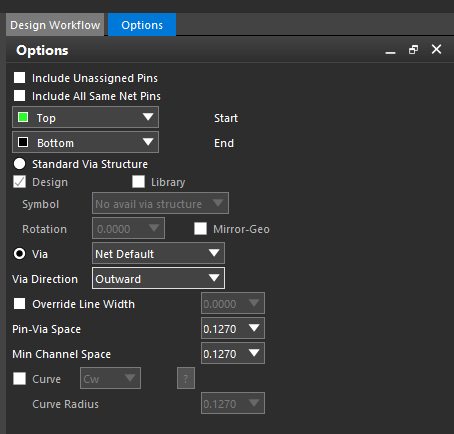
- In the Options tab, set the Via Direction to Outward.
- Click on the components with both pins connected to either ground or power.
- In the Find tab, uncheck Symbols.
Note: This will select and fanout only individual pins.
- Click to fanout the remainder of the ground and power pins.
Note: There is no need to fanout power or ground pins on JP1 or JP2.
- Right click and select Done.
- Select the Setup > Application Mode > Etch Edit from the menu.
- Click on a DRC marked trace on IC1 and drag to move the via and trace on the inside of the IC.
- Complete this for all the DRC error traces on IC1.
- Select Edit > Change Objects from the menu.
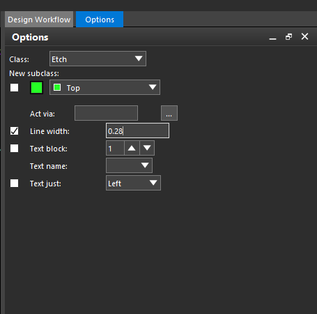
- Select Line width and assign a value of 0.28.
- Click on all the traces routed for IC1 to change the width.
- Right click and select Done.
Note: The DRC errors are now resolved, and the markers have been removed.
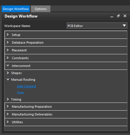
- In the Design Workflow, select Interconnect > Manual Routing > Add Connect.
- Click each connection to place a trace.
- Route the PCB.
Note: In the Options tab, you can set the angle of the trace, change the line width, choose to shove or hug a trace, shove vias, smooth traces and auto blank all other rats. Click on one of the traces for the differential pair and they will be routed together. To add vias, right click and Add Via at any point during your trace. If you make mistake while routing, right click and select Oops.
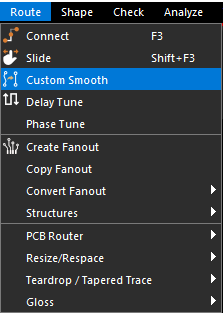
- Select Route > Custom Smooth from the menu.
- Click on the trace you would like to smooth or highlight a selection
Note: OrCAD PCB Designer will automatically smooth the trace.
- Select Route > Slide from the menu.
- Click on the segment you want to slide and click to place.
- Right click and select Done.
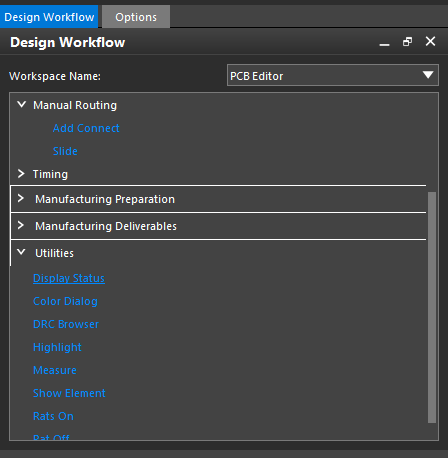
- In the Design Workflow, select Utilities > Display Status.
- Ensure all the nets and connections are routed.
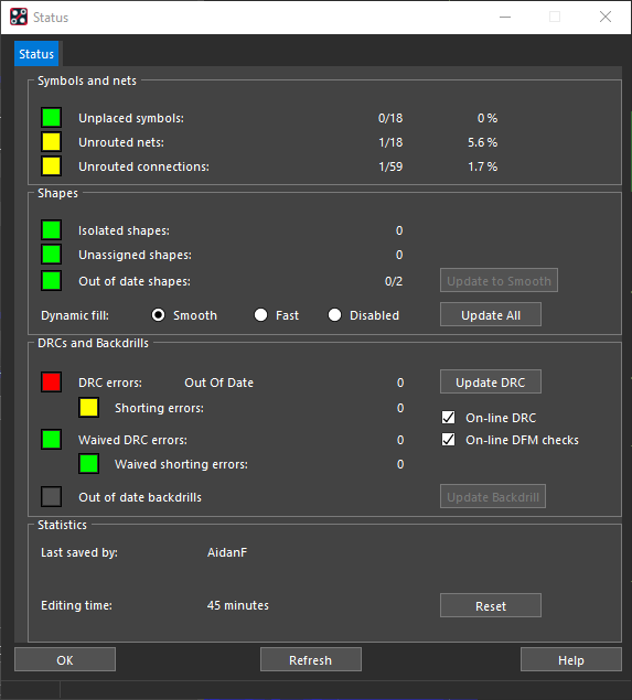
Note: If all nets and connections are routed, the corresponding buttons will be color-coded green. If any nets or connections are unrouted, the corresponding buttons will be color-coded yellow. To resolve the unrouted connections, use the following steps:
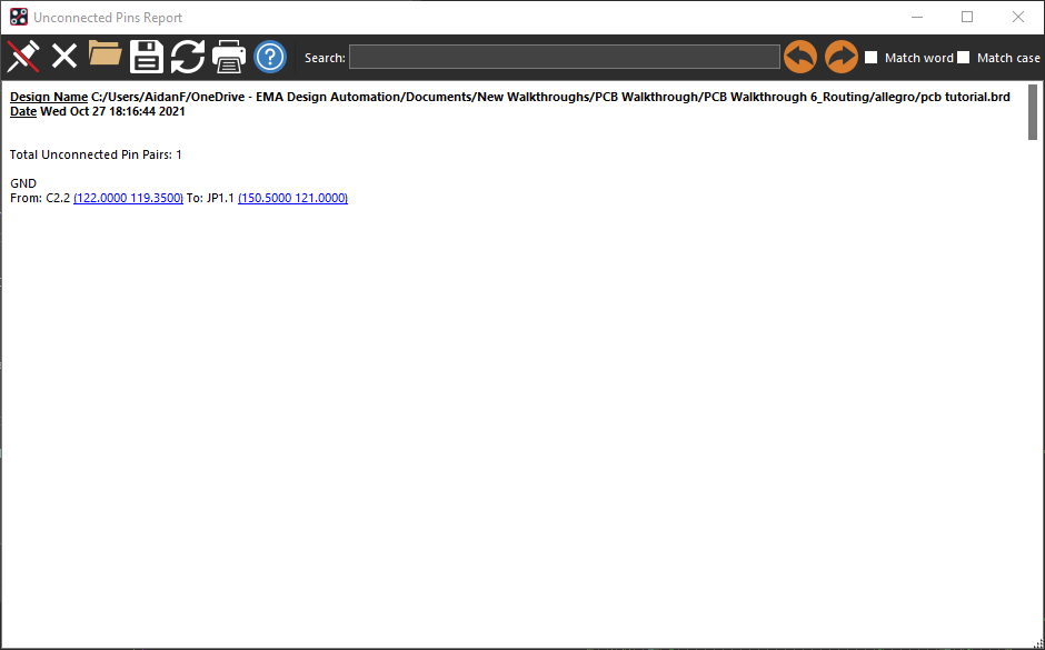
- Select the button next to Unrouted Connections. This will activate the Unconnected Pins Report which displays the pin pairs that are not connected.
- Select a coordinate to be brought to the location on the PCB.
- Close the Display Status window.
- Route the unrouted connection(s).
- Select Utilities > Display Status from the Design Workflow to confirm all nets and connections are routed.
- Close the Display Status Window.
