PCB Walk-through 8: Manufacturing Preparation
This walk-through demonstrates how to prepare your board for manufacturing and generate manufacturing data. After you complete this topic, you will be able to:
- Add dimensions and titleblock for fabrication
- Create a Drill Chart and Cross Section Chart
- Setup Artwork Films
To follow along, continue working with the design completed in PCB Walkthrough 7 or open the provided board file in the folder directory, PCB Walkthrough 8_Manufacturing Preparation.
If design files were not downloaded in the beginning of the walk-through, they can be accessed through the Materials tab above.
 Open in New Window
- Select the Color button from the toolbar.
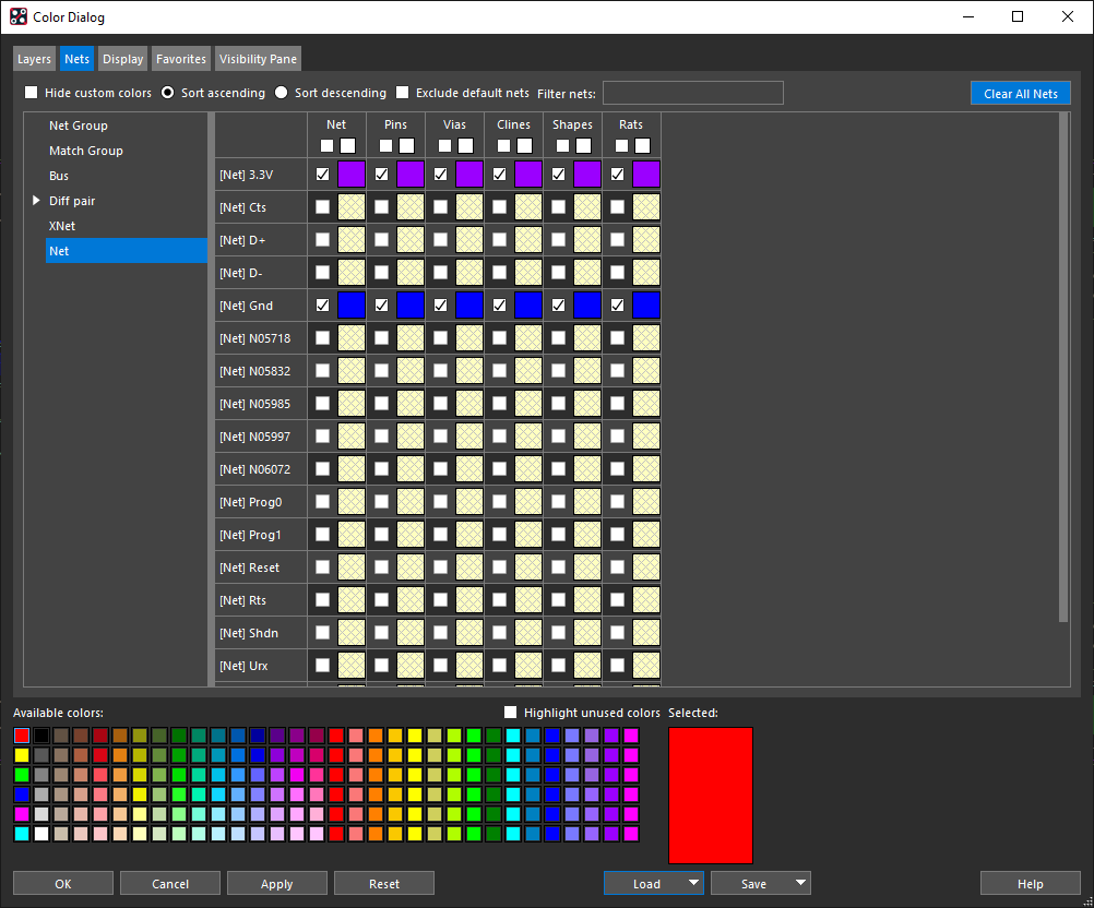
- Select the Nets tab and select Clear all Nets.
- Select Yes to clear the nets and click OK.
- Select Setup > Application Mode > General Edit from the menu.
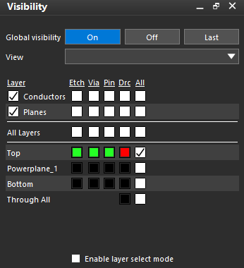
- In the Visibility tab, set Global Visibility to On.
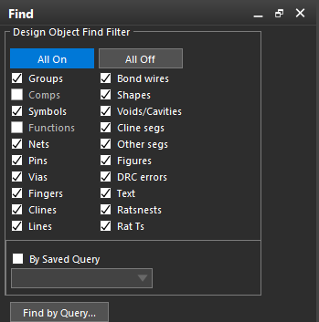
- In the Find tab, select All On.
- Highlight the board.
- Select the Move button on the toolbar.
- Click the canvas to place your board at a new location.
- Zoom in to the bottom of the board.
- Select Setup > Change Origin from the menu.
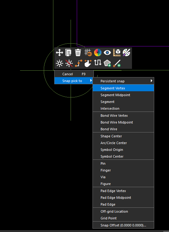
- Right click the corner of the board and select Snap Pick to > Segment Vertex.
- Select Place > Component Manually from the menu.
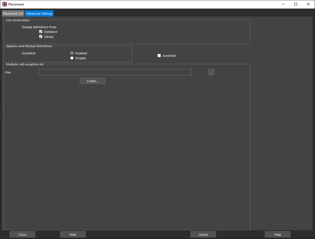
- In the Advance Settings tab, select Library.
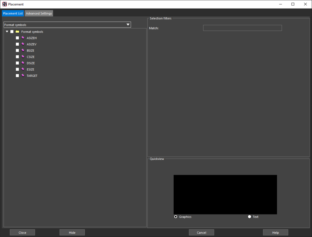
- In the Placement List tab, select Format symbols from the drop-down.
- Select the box next to ASIZEH.
- Click the canvas to place.
- Close the placement window.
- Select Add > Text from the menu.
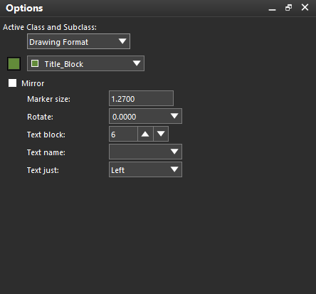
- In the Options tab, select Drawing Format and Title_Block as the Active Class and Subclass.
- Set the Text Block to 6.
- Click the canvas and type the desired text.
- Right click and select Done.
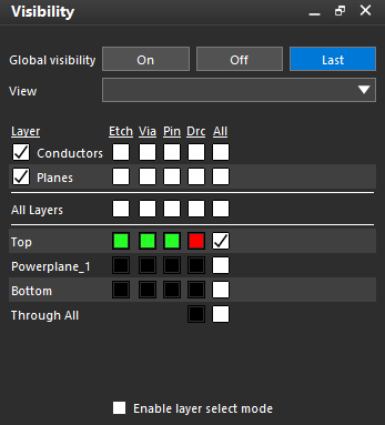
- In the Visibility tab, select Last.
- In the Find tab, select All Off then select Text.
- Edit the text on the board as needed.
Note: To delete, right click and select delete. To move, click and drag. To rotate select the text, right click and choose spin.
- Select Edit > Change Object from the menu.
- Uncheck the line width box and select Text Block.
- Change the Text Block to 2.
- Click on the reference designator text for each component or highlight the design to select all reference designators.
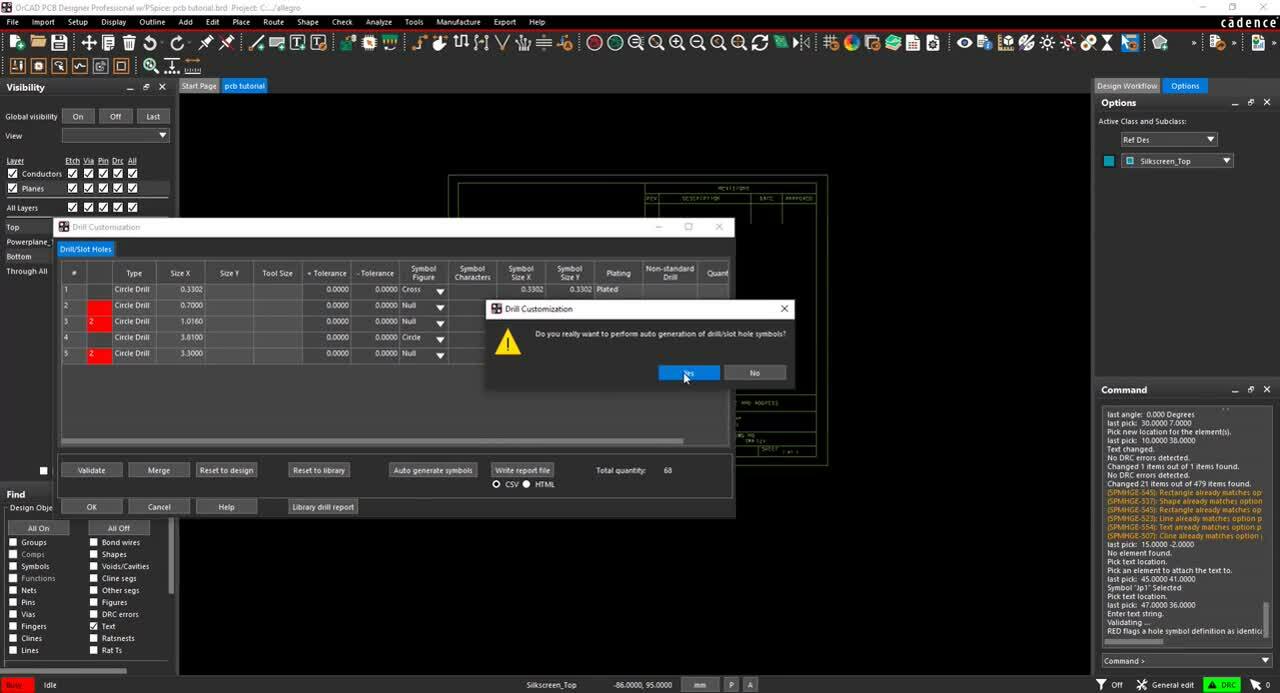
- Select Manufacture > Customize Drill Table from the menu.
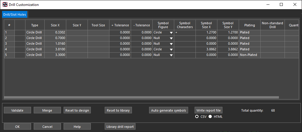
- Select Validate.
- Select Auto generate Symbols and Yes. Click OK.
- In the Design Workflow, select Manufacturing Preparation > Documentation > Drill Chart.
- Leave the defaults and click OK to create drill chart.
- Click the canvas to place the drill chart.
- In the Design Workflow, select Manufacturing Preparation > Documentation > Cross Section Detail.
- Set the Text Block to 3.
- Click OK and click the canvas to place.
- Select Manufacture > Dimension Environment from the menu.
- Right click and select Linear Dimension.
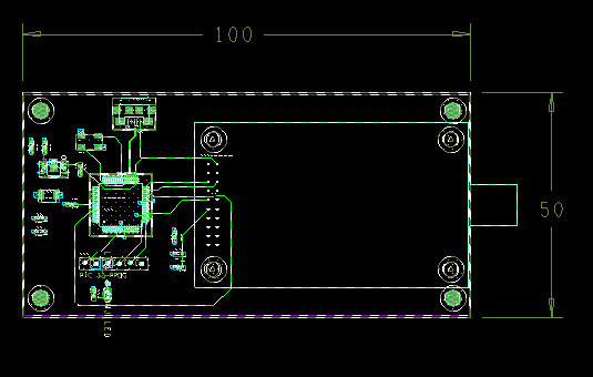
- Click corners of the board to dimension. Click to place the dimension.
- Right click and select Done.
- Select Setup > User Preferences from the menu.
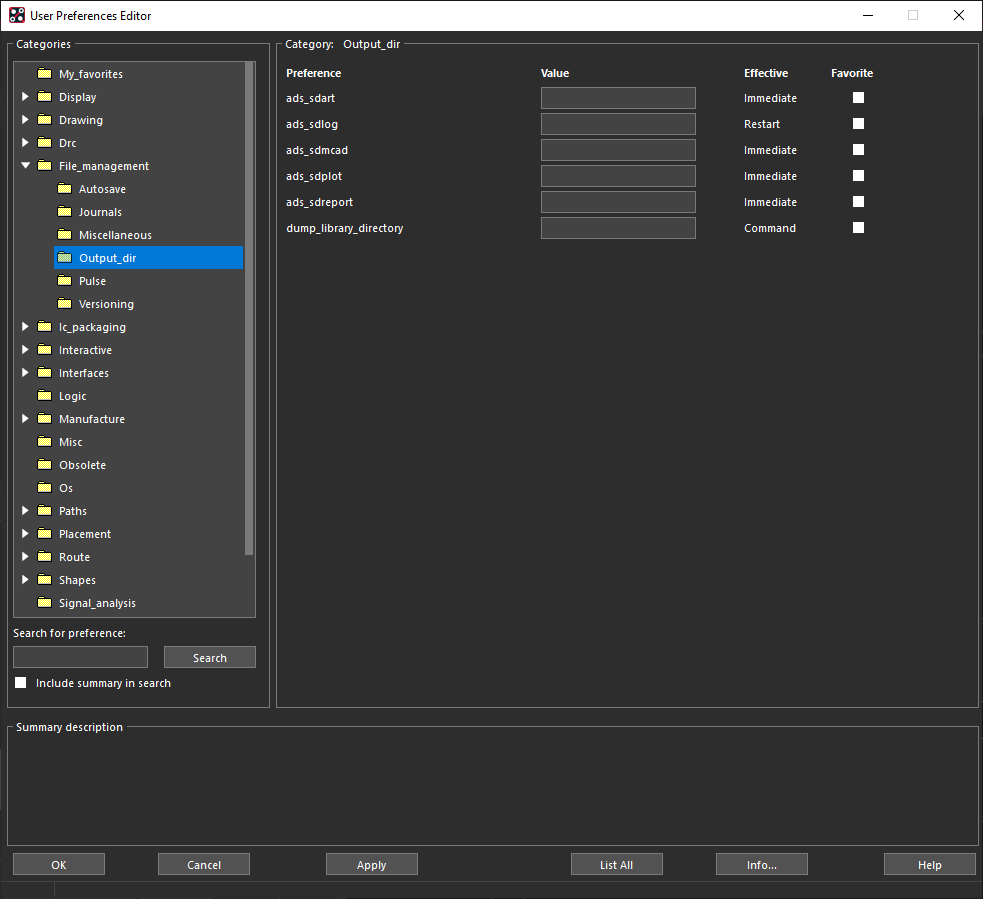
- Select File_management > Output_dir.
- Add the text .artwork to the first input field. Click OK.
Note: This will create a folder for your exported artwork.
- Select the Color button from the toolbar.
- Select Off for Global Visibility.
Note: This will turn off all layers and ensue only the necessary layers are selected.
- In Drawing Format, select All.
- In Manufacturing, select NClegend1-3 and Xsection_Chart.
- In Geometry, select Design_Outline and Dimension.
- Select Apply.
- In the Design Workflow, select Manufacturing Preparation > Documentation > Artwork (Film Records) Setup.
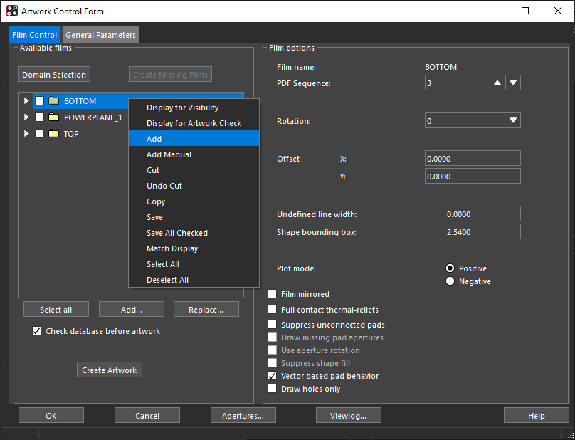
- Right click on one of the entries in the film window and select Add.
- Assign FAB as the film name and click OK.
- Change the Undefined line width to 0.127.
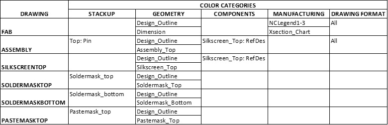
- Complete this process for all the Artwork Films using the provided table below:
Note: If you need to make changes to existing films, expand the film name. Add or cut layers as needed. To view a film in the PCB Window, right click and select display for visibility or in the Visibility Tab, select from the films in the drop-down.
- Close the Artwork setup window and the Color window.
