Capture Walk-through 6: Part Information
This walk-through demonstrates how you can add and edit design part information either before or after part placement. After you complete this topic, you will be able to:
- Edit component values and display information on the schematic
- Add PCB footprints to your design
To follow along with this tutorial, continue with your design from Capture Walk-through 5 or use the included design file, CAPTURE TUTORIAL 6_PART INFORMATION.DSN under the ‘materials’ tab.
 Open in New Window
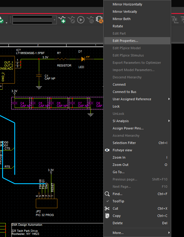
- Select all the VCC components. Right click and select Edit Properties.
Note: To select multiple components, hold down the CTRL key on the keyboard.
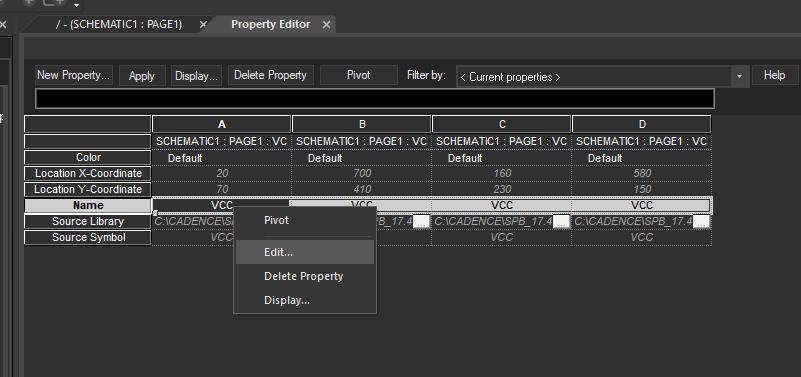
- In the Property Editor window, select the Name row. Right click and select Edit.
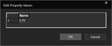
- Add 3.3V and click OK.
- Close the properties window.
Note: You can also assign the value during placement. Select Place > Power from the menu. Select VCC and OK. Before placing right click and select Edit Properties. Add 3.3V for the value and click OK. Now the component will be placed with the correct value.
- Highlight the section of series capacitors. Right click and select Edit Properties.
Note: In the Property Editor, make sure to select the Parts tab.
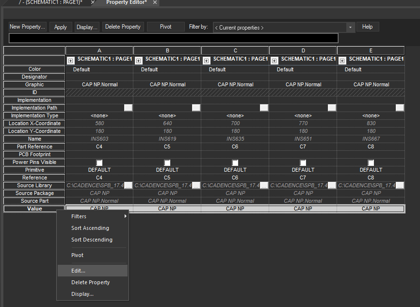
- Right click the Value row and select Edit.

- Add 0.1uF and click OK.
- Close the properties window.
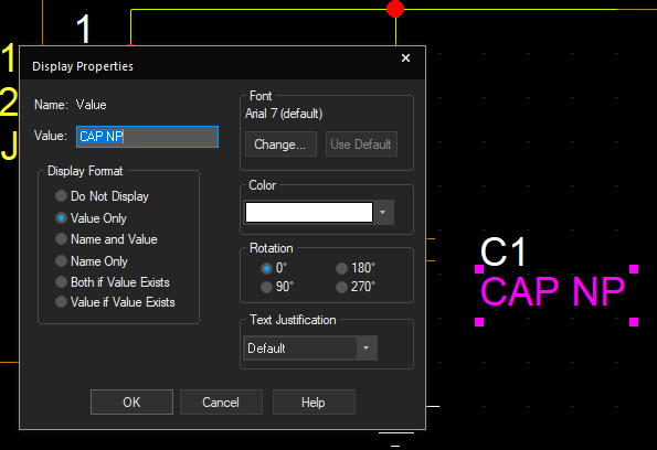
Note: You can also activate the properties window by double clicking a component. Double click on text to change the value. You can change the Display Format in the Display Properties window.
- Finish adding the component values according to the provided Capture Tutorial.PDF file.
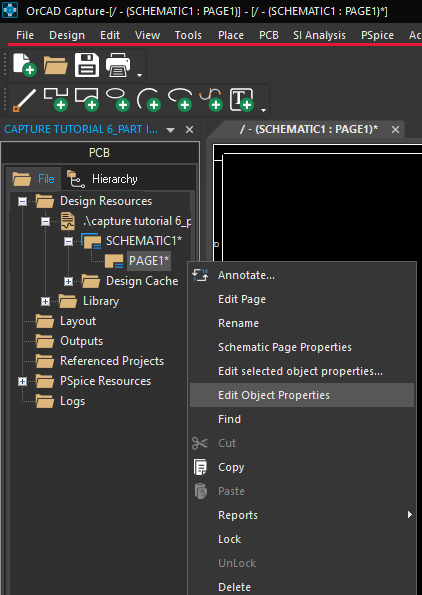
- In the project hierarchy, right click on PAGE1 of the schematic and select Edit Object Properties.
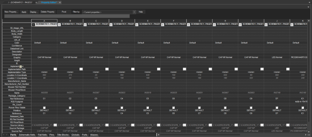
Note: This will display the properties for all the components placed on Page 1 of the schematic. Footprints have not been assigned for capacitors, resistors, or the LED. Parametric information for the part placed through the Unified Search (Capture Walk-through 3: Placing Parts), has been automatically populated.
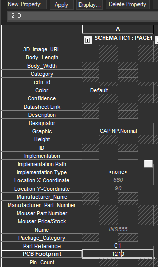
- Assign the footprint name 1210, for capacitor C1.
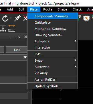
Note: If the footprint name is unknown, Open OrCAD PCB Designer. Select Place > Components Manually from the menu.
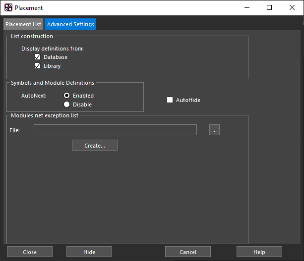
Select the Advanced Settings tab and check Library.
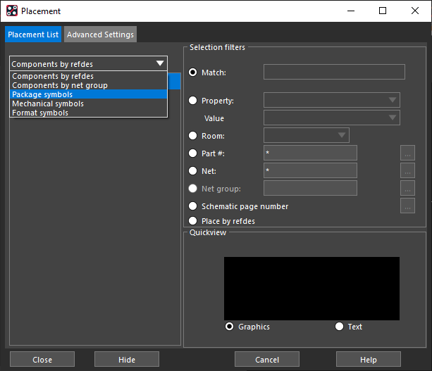
Return to the Placement List tab and select Package Symbol from the drop-down menu.
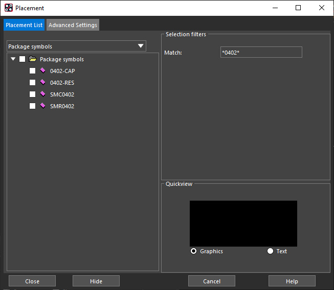
Search for *0402* and press Enter on the keyboard. This will return any footprint with 0402 in the name. Check the box next to the name to preview the 0402-CAP footprint.
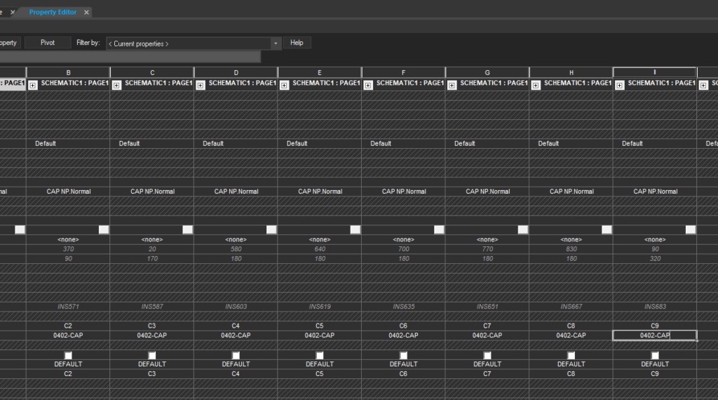
- Assign 0402-CAP as the PCB Footprint for the remaining capacitors.
Note: You can use the keyboard shortcuts CTRL+C and CTRL+V to add footprints
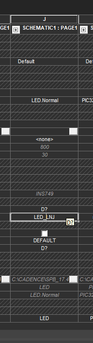
- Back in the schematic properties window, assign LED_LNJ as the footprint name for the LED.
- Assign the footprint 0402-RES to all resistors.
- Close the Properties Window.
- In the schematic, right click on a component and select Show Footprint.
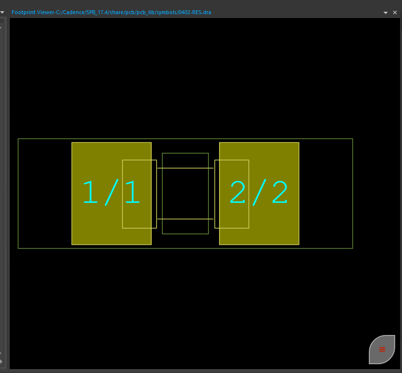
Note: This will allow you to verify the footprint in the Footprint Viewer.