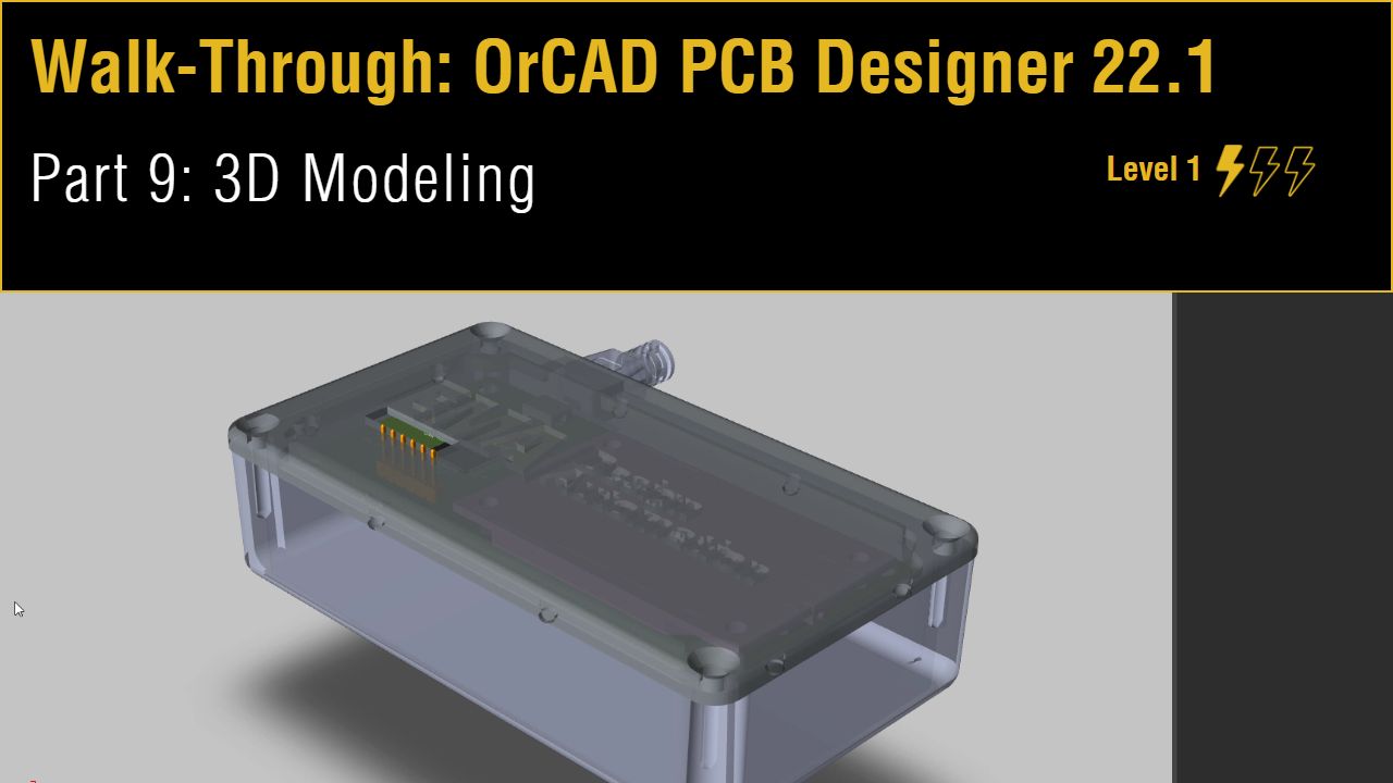
Lesson 9: 3D Modeling
This walk-through demonstrates complete STEP Model mapping and collision detection within the 3D Canvas in OrCAD PCB Designer 22.1 (2022). After you complete this topic, you will be able to:
- Map 3D Models to PCB footprints
- Add mechanical housing and models
- Perform collision detection
- Cross-probe between 2D and 3D to resolve collisions
To follow along, continue with the design from the previous lesson or use the downloaded materials.
If materials were not downloaded at the start of the walk-through, they can be accessed in the Materials tab of this lesson.
 Open in New Window
Adjusting Visibility
Step 1: Select Setup > Colors from the menu or the Color192 icon from the toolbar.
Step 2: Select the Layers tab and the Stack-Up color list.
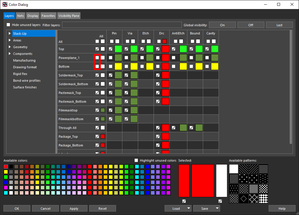
Step 3: Check All and uncheck Powerplane_1 and Bottom.
Step 4: Select the Areas list. Check All.
Step 5: Select the Geometry list. Check All and uncheck Dimension.
Step 6: Select the Components list. Check All.
Step 7: Select the Manufacturing list. Check, then uncheck All to turn visibility off.
Step 8: Select the Drawing Format list. Check, then uncheck All.
Step 9: Click OK to close the Color Dialog window.
Mapping 3D Models
Step 10: Select Display > 3D Canvas from the menu or the 3D button from the toolbar.
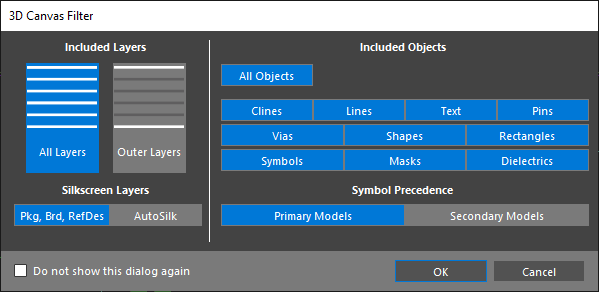
Note: When first selecting the 3D Canvas, the 3D Canvas Filter will be activated. Here you can select which portions of the design are included in the 3D representation. Within the 3D canvas, you can select which layers are visible in the visibility tab. You can select which models are visible in the symbols tab. By default, any components without 3D models are represented with a boundary shape. To change this, select Setup > Preferences > Symbol Representation and select the desired display for each symbol.
Step 11: Select the 3D Mapper tab in the 3D canvas.
Step 12: Select Footprint under Map To.
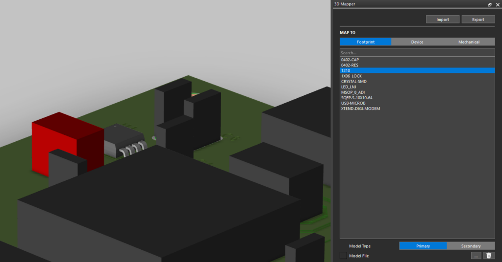
Step 13: Select 1210 from the list.
Step 14: Select Primary as the Model Type. Click the ellipsis to load a Model File.
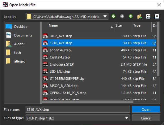
Step 15: Browse to the 3D Models folder and select 1210_AVX.step. Click Open.
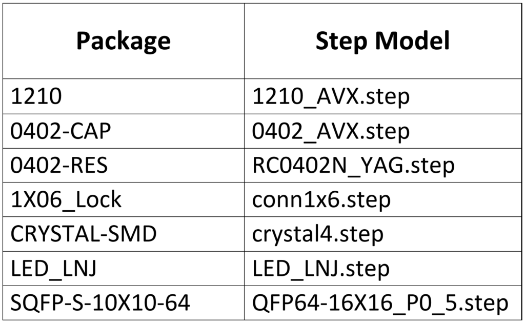
Step 16: Complete the STEP mapping for all components using the table below:
Note: No adjustments need to be made for these step models as they are automatically aligned to the PCB footprints. MSOP_8_ADI has been mapped already.
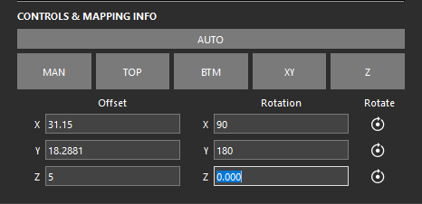
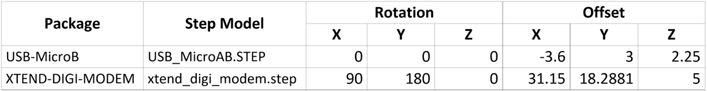
Step 17: Complete the STEP Mapping for the following components by adjusting the rotation and offset according to the table below:
Note: The 3D Mapper includes several options for quick and efficient model mapping including automatic mapping, manual mapping, mapping to the top or bottom of the board, and more. Learn more with this how-to.
Step 18: Select Mechanical under Map To.
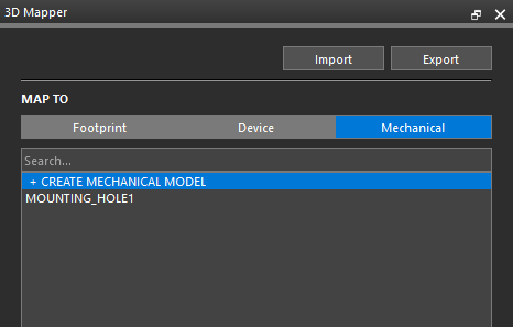
Step 19: Double-click Create Mechanical Model.
Step 20: Double-click the name of the newly created model to change it. Enter the name STEP3D_MECH_USB. Press Enter on the keyboard.
Step 21: Map USB.step to the new mechanical package using the table below:

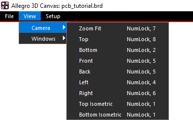
Note: Select View > Camera from the menu to change the view and ensure the STEP file is mapped correctly. To rotate the board in the 3D Canvas, hold down the SHIFT key on the keyboard and press the middle mouse button. Alternatively, you can choose preset views by selecting View > Camera from the menu.
Step 22: Double-click Create Mechanical Model.
Step 23: Name the model STEP3D_MECH_ENCLOSURE.
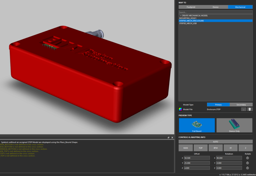
Step 24: Map Enclosure.STEP to the new mechanical package using the table below:

Note: To turn visibility on/off for mechanical symbols and components in the design select View > Windows > Symbols from the menu. To adjust the transparency of the mechanical models, select Setup > Preferences > Symbol Representation from the menu.
Calculating Collisions
Step 25: Select the Collision Detection tab in the 3D Canvas.
Note: If this tab is not visible, select View > Windows > Collision Detection from the menu.
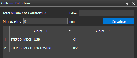
Step 26: Select Calculate. Two collisions are listed:
- Between JP2 and the enclosure
- Between X1 and the USB connector
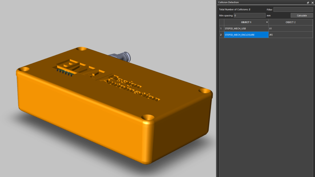
Step 27: Select STEP3D_MECH_ENCLOSURE to highlight the enclosure and collision in orange.
Step 28: Right-click the listing and select Locate. The component will flash for easy detection.
Using the Cutting Plane
Step 29: Right-click the canvas and select Cutting Plane.
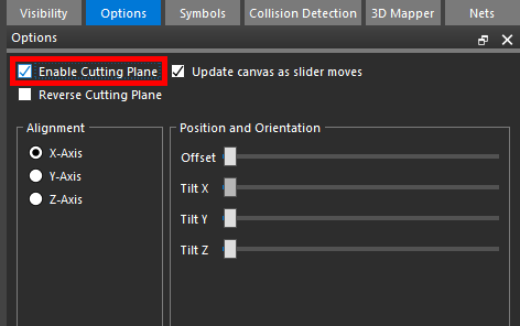
Step 30: Check Enable Cutting Plane.
Note: The Cutting Plane can be used to view a cross section of the PCB to help determine collision and design structure issues.
Step 31: Adjust the Offset, Tilt X, Tilt Y, and Tilt Z sliders to adjust the offset and tilt of the cut for more detail.
Step 32: Uncheck Enable Cutting plane, then right-click and select Done to return to normal mode.
Cross-Probing with the PCB
Step 33: Select Setup > Preferences from the menu.
Step 34: Select Interactive from the Categories list.
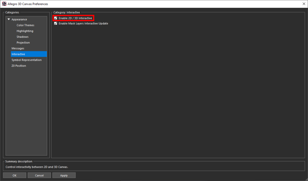
Step 35: Check Enable 2D/3D Interactive and click OK.
Step 36: Set up a split screen between the PCB canvas and the 3D canvas.
Step 37: In OrCAD PCB Designer, ensure Symbols is selected in the Find panel.
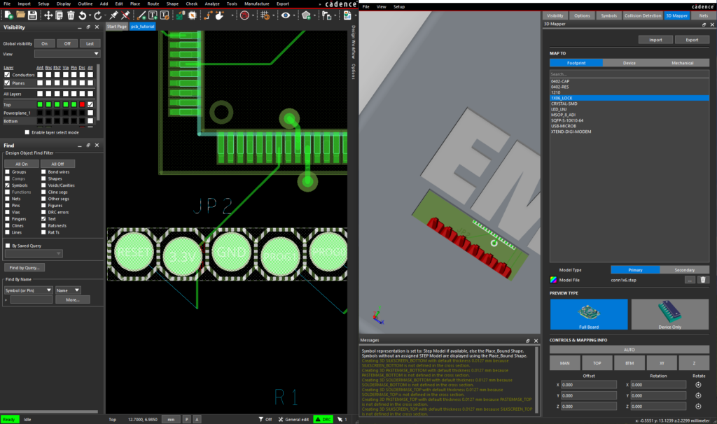
Step 38: Click and drag the connector JP2 to line up with the existing cutout in the enclosure. The changes will appear automatically in the 3D view once the part is placed.
Step 39: Re-route the connections.
Note: Delete the existing traces. Select Route > Connect from the menu and click to place the trace. Right-click and select Done when finished. Add custom smoothing as needed.
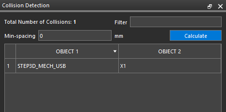
Step 40: Back in the 3D canvas, select the Collision Detection tab and select Calculate. The errors have been resolved and only the collision between X1 and the USB connector is reported.
Exporting a 3D PDF
Step 41: In the PCB canvas, select File > Save from the menu or select the Save button from the toolbar. Click Yes to overwrite the design.
Step 42: In the 3D canvas, select File > Export from the menu.
Step 43: Select PDF 3D from the Files of Type dropdown.
Step 44: Name the file and click Save.
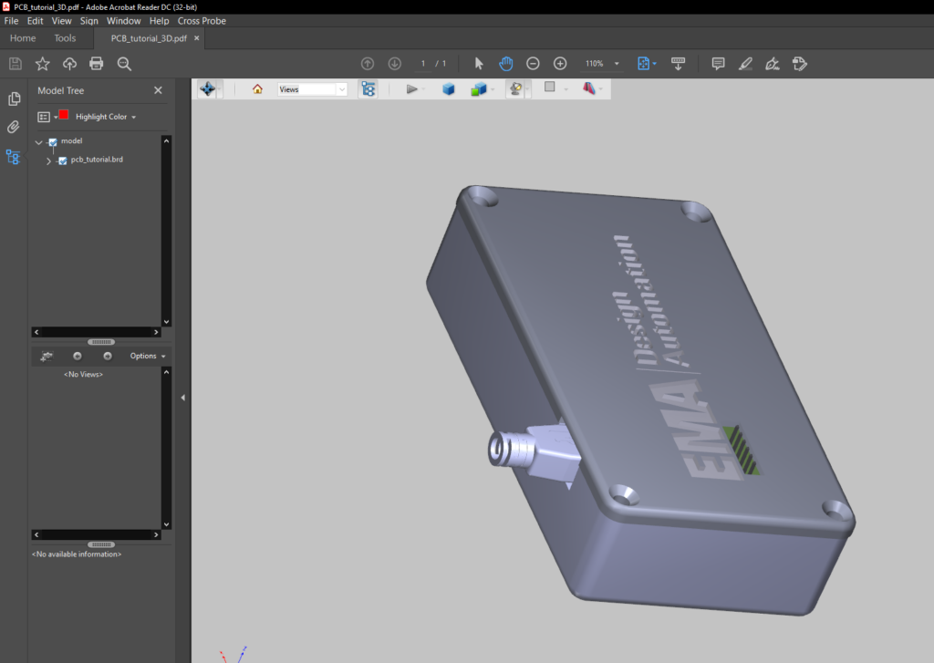
Note: The 3D PDF can be viewed in a PDF viewer such as Adobe Reader.