To guarantee end product success and integration with mechanical housing, a realistic representation of the board and components is required. OrCAD PCB Designer includes a quick and seamless method to map 3D models, with features including:
- Direct access through the 3D canvas
- Automatic mapping
- Multiple options for accurate and efficient mapping
- Support for STEP Models, mechanical parts, and mechanical housing
This how-to will provide step-by-step instructions on how to automatically and manually map 3D Models to footprints and mechanical parts using OrCAD PCB Designer.
How-To Video
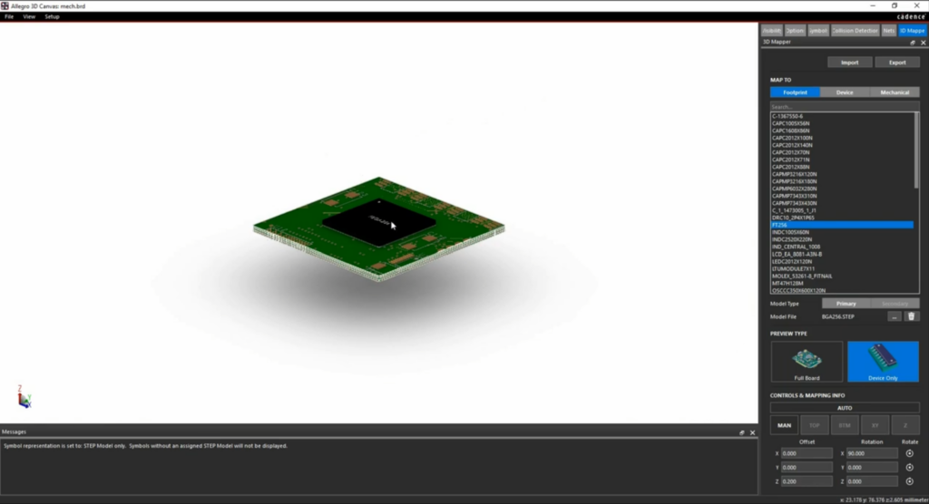
Automatically Mapping a 3D Model
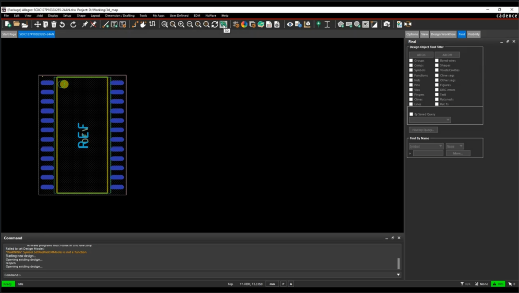
Step 1: Open a PCB Footprint (.dra) in OrCAD PCB Designer.
Step 2: Select Display > 3D Canvas from the menu or the 3D Canvas button on the toolbar.
Step 3: In the 3D Canvas, select the 3D Mapper tab.
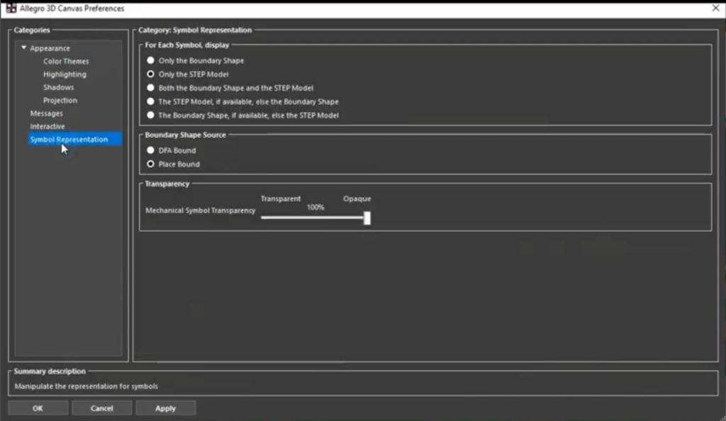
Note: If the 3D Mapper window is not visible, select View > Windows > 3D Mapper. If you are receiving an error in the 3D Mapper window, select Setup > Preferences > Symbol Representation. Make sure one of the following options is selected:
- Only the STEP Model
- Both the Boundary Shape and the STEP Model
- The STEP Model, if available, else the Boundary Shape
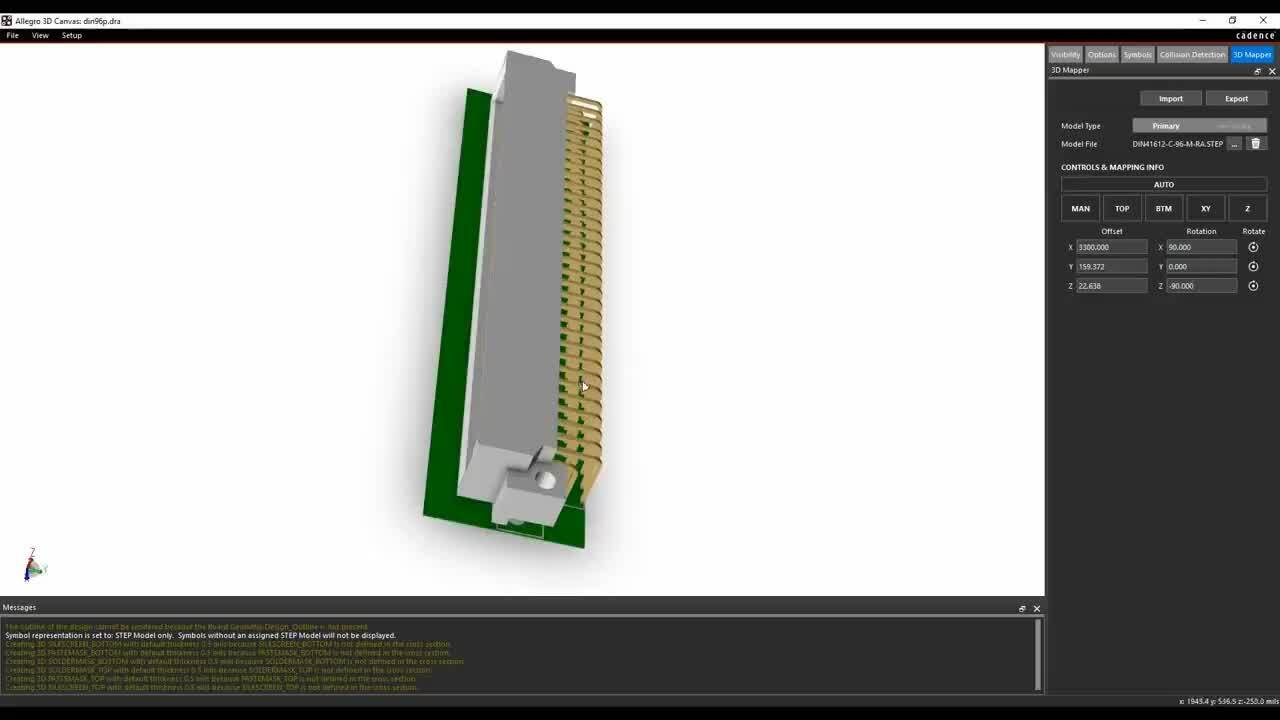
Step 4: Under Model File, select the ellipses and browse for the appropriate STEP Model. Click Open.
Note: Other formats are now compatible for 3D Mapping, including SOLIDWORKS, Autodesk Inventor, Creo, ACIS, and more.
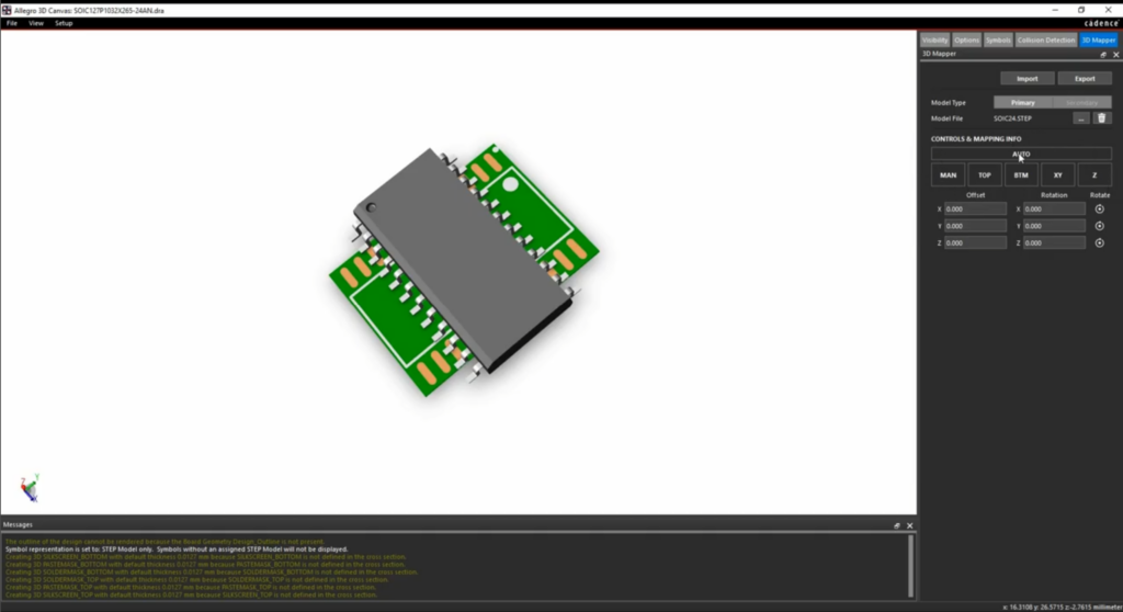
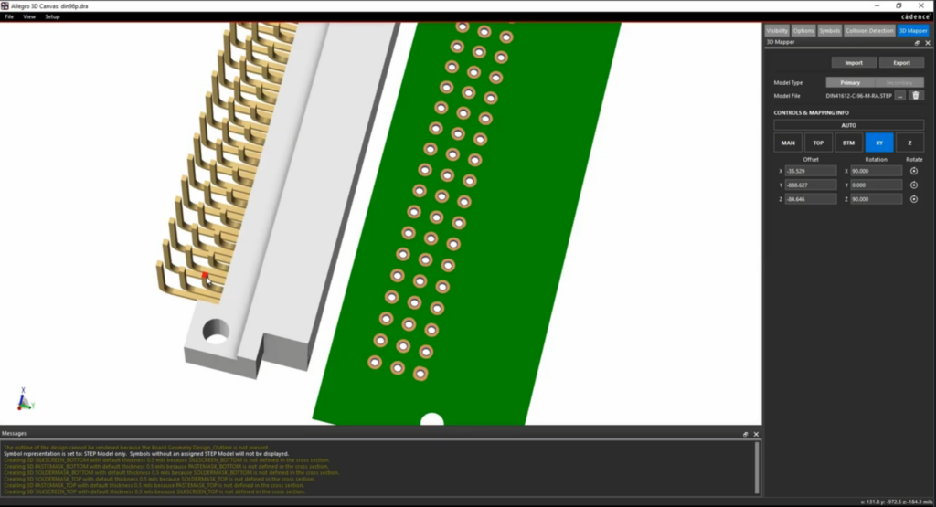
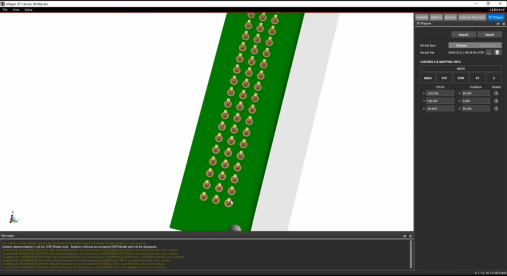
Step 5: Select AUTO.
Note: By Selecting Auto, OrCAD PCB Designer automatically maps the 3D Model to the PCB footprint.
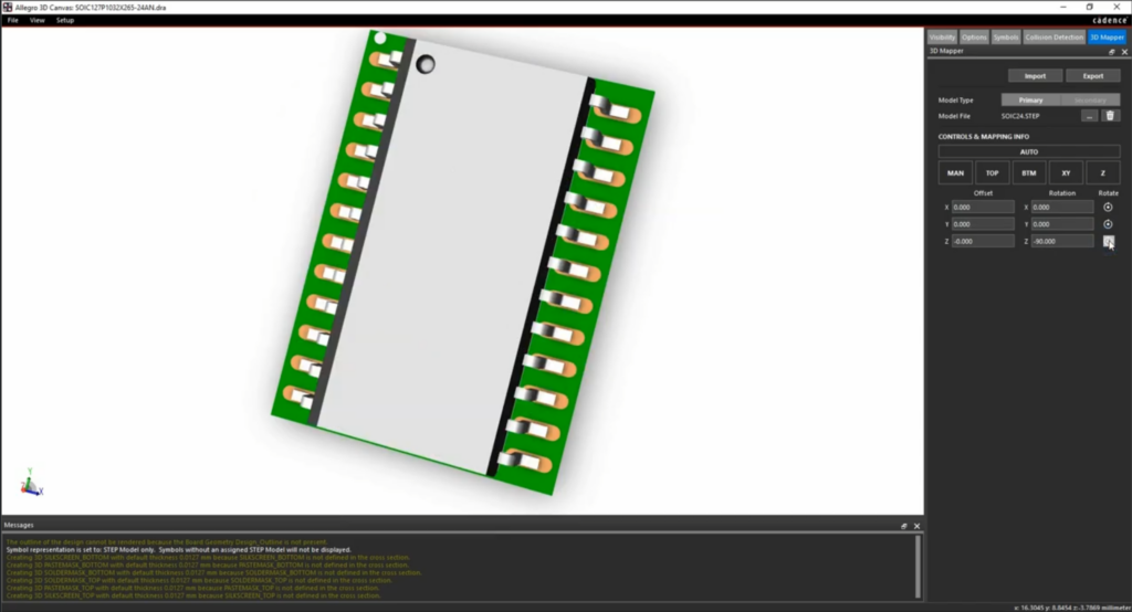
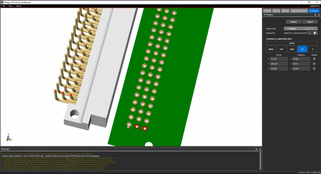
Step 6: In the Z-axis, click Rotate twice to align pin 1 of the 3D Model with pin 1 of the PCB footprint.
Step 7: Close the 3D Canvas. Select File > Save or the Save button on the toolbar to save the PCB Footprint.
Note: When 3D Models are mapped to the PCB footprint file, any design utilizing that PCB footprint will have the 3D Model already attached.
Other 3D Mapping Options
Step 8: Open a PCB Footprint (.dra) in OrCAD PCB Designer.
Step 9: Select Display > 3D Canvas from the menu or the 3D Canvas button on the toolbar.
Step 10: In the 3D Canvas, select the 3D Mapper tab.
Step 11: Under Model File, select the ellipses and browse for the appropriate STEP Model. Click Open.
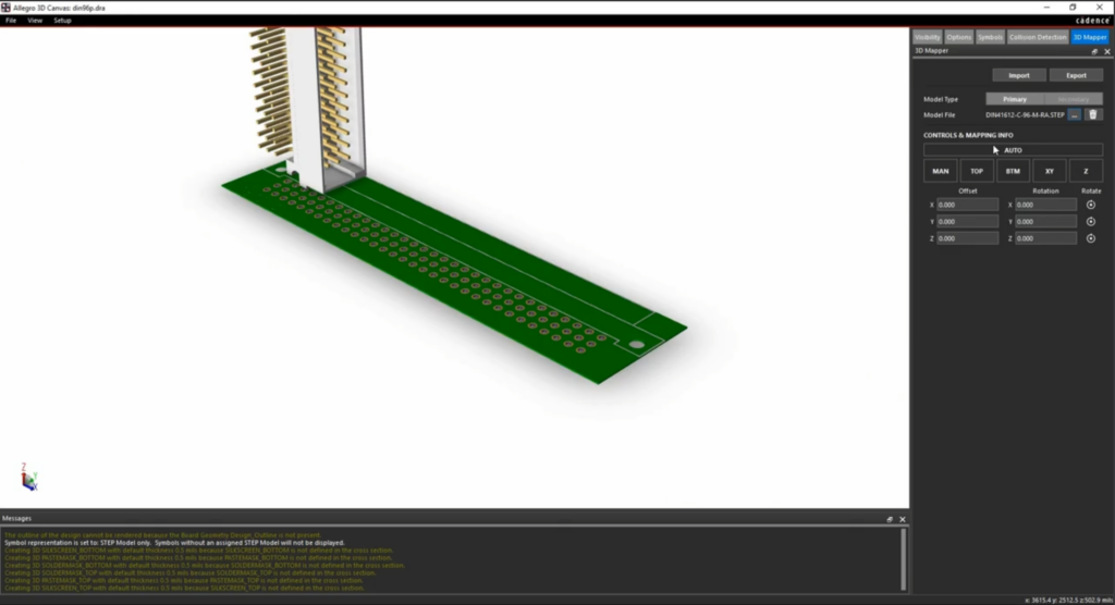
Step 12: Select AUTO.
Step 13: In the Z-axis, click Rotate twice to align the 3D Model to the PCB footprint.
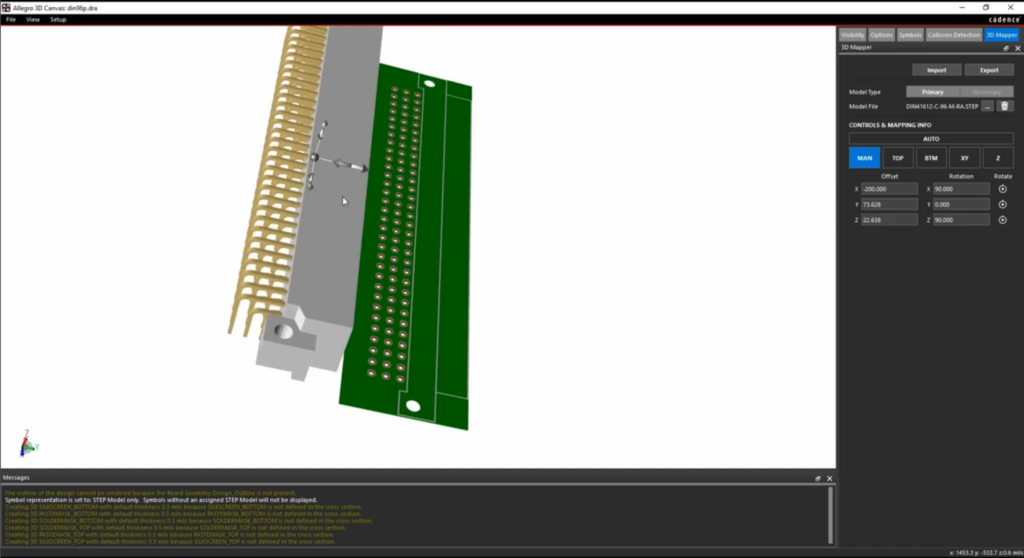
Step 14: Select MAN.
Note: Selecting Manual will activate a drag handle allowing you to drag and adjust the model’s location in the 3D Canvas.
Step 15: Select TOP.
Note: Selecting Top will activate mapping for the top face of the 3D Model to the PCB footprint. Selecting Bottom (BTM) will activate mapping the bottom face of the 3D Model to the PCB footprint.
Step 16: Select the top face of the 3D Model.
Step 17: Select XY.
Note: This option will map a pin to a hole in the PCB and requires at least 2 pins to complete the mapping.
Step 18: Select the pin surface on the 3D Model.
Step 19: Select the corresponding hole surface on the PCB footprint.
Note: Make sure to select the pins and holes in the same order for footprints and 3D Models to be mapped properly.
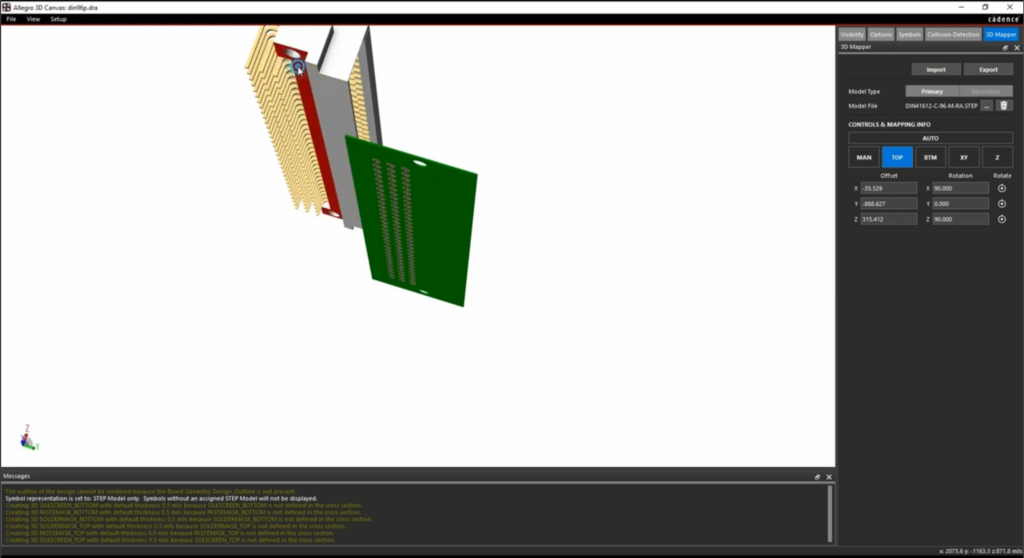
Step 20: Select XY.
Step 21: Close the 3D Canvas. Select File > Save or the Save button on the toolbar to save the PCB Footprint.
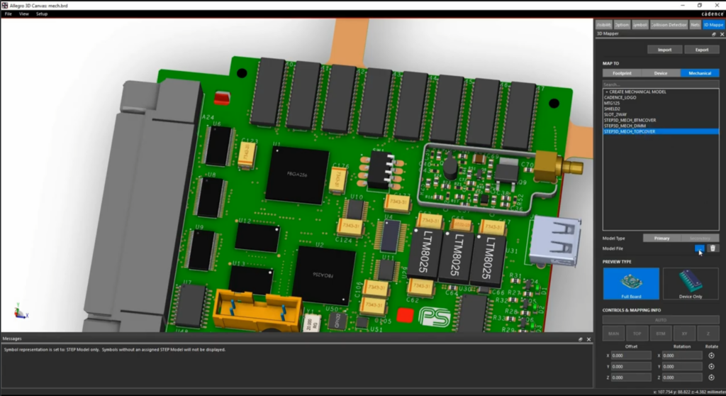
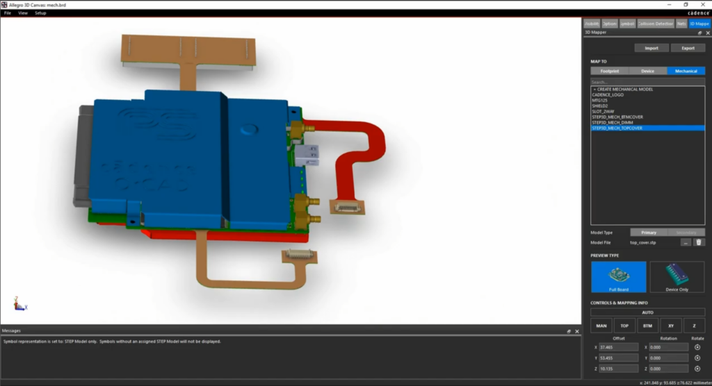
Incorporating Mechanical Housing
Step 22: Open a Board File (.brd) in OrCAD PCB Designer.
Step 23: Select Display > 3D Canvas from the menu or the 3D Canvas button on the toolbar.
Step 24: In the 3D Canvas, select the 3D Mapper tab.
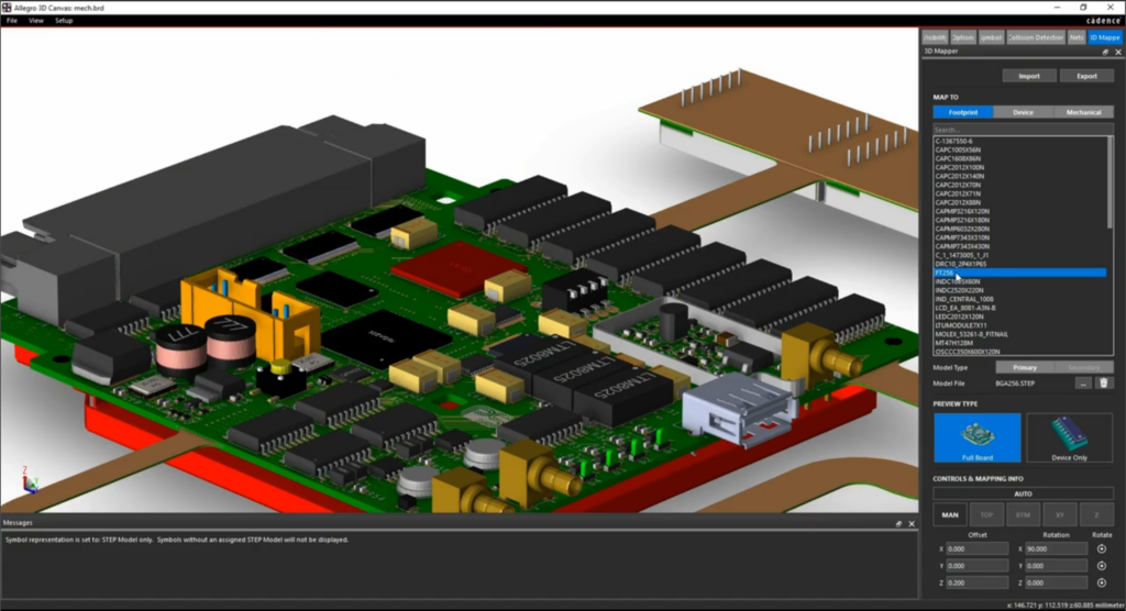
Step 25: Under MAP TO, select Footprint. Click on a desired component from the list.
Note: The corresponding symbol is highlighted in the 3D Canvas for review. To review only the selected component and the 3D Model, select Preview Type > Device Only.
Step 26: Under MAP TO, select Mechanical.
Note: This tab is used to map mechanical models such as covers, shields, and housing. To create a new mechanical aspect in the design, select Create Mechanical Model.
Step 27: Select STEP3D_MECH_TOPCOVER.
Step 28: Under Model File, select the ellipses and browse for the appropriate STEP Model. Click Open.
Step 29: Select TOP.
Step 30: Select the top of the cover.
Step 31: Select MAN and drag the cover away from the PCB.
Step 32: Select XY.
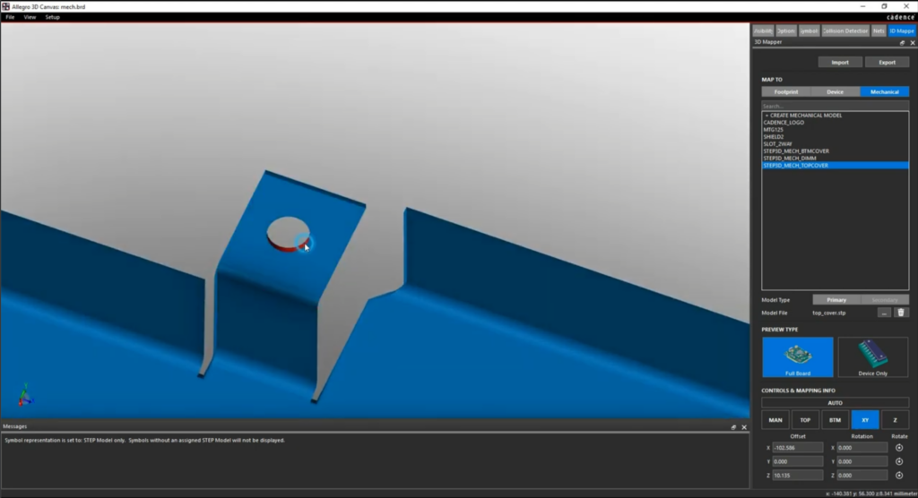
Step 33: On the 3D Model of the cover, select the inside surface of two holes.
Step 34: On the PCB, select the corresponding holes to map to in the same selection order.
Step 35: Select XY.
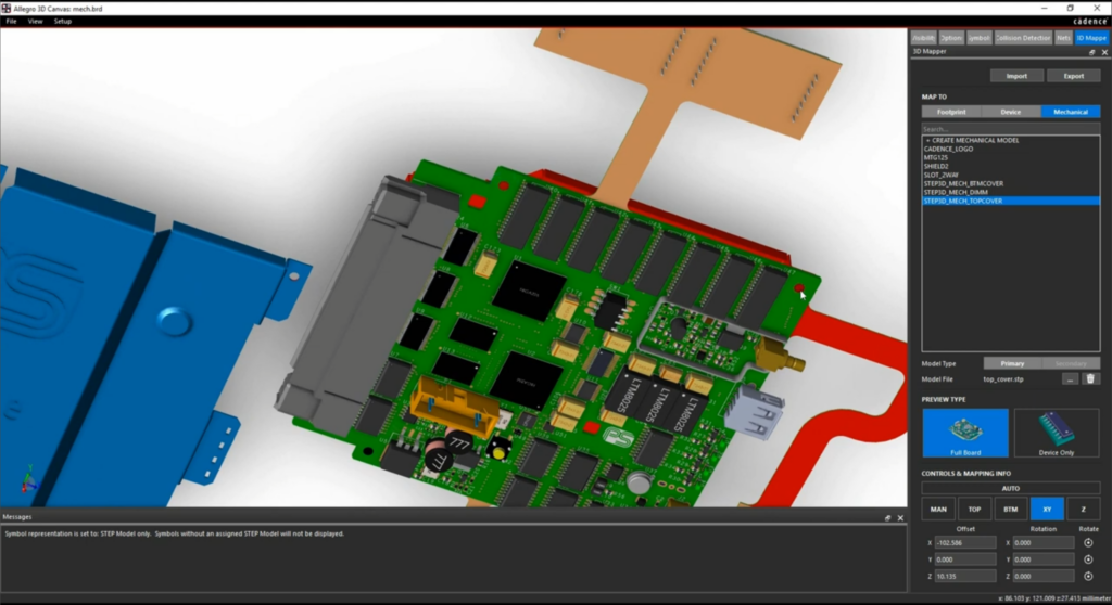
Step 36: Close the 3D Canvas. Select File > Save or the Save button on the toolbar to save the design.
Wrap Up & Next Steps
Quickly and efficiently map 3D Models for components and mechanical housing to ensure overall design success with a realistic representation of the end product. For more information on the latest OrCAD updates, be sure to visit our release page and upgrade your license to take advantage of the new 3D mapping functionality.

