With design speeds increasing, it’s critical to analyze signal quality throughout the design process. Identifying signal integrity issues AFTER PCB production can lead to a complete redesign and have a detrimental effect on the project budget and timeline. Quickly find and fix problematic traces during the PCB layout, with real-time impedance and coupling analysis in OrCAD PCB Designer Professional.
This how-to will show:
- How to perform signal integrity analysis during a PCB Design
- How to use the Impedance and Coupling Workflows in OrCAD PCB Designer Professional
- How to identify impedance and coupling issues
- How to analyze tables and overlay results of the impedance and coupling simulation
- How to resolve common signal integrity issues
To follow along with this tutorial, download the provided files above the table of contents.
How-To Video
Activating Real-Time Analysis
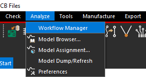
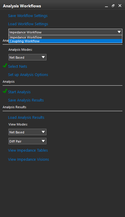
Step 1: In OrCAD PCB Designer Professional, open the Workflow Manager by selecting Analyze > Workflow Manager from the menu.
Step 2: From the workflow drop-down menu, select the Impedance Workflow.
Note: The Analysis Workflow Manager will walk through the necessary steps and settings to perform the desired analysis.
Configuring Impedance Analysis
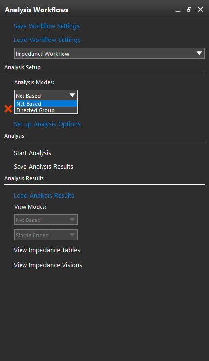
Step 3: Under Analysis Modes select Net Based.
Note: The following options are available for analysis:
- Net Based: Allows every segment of selected nets or all nets to be simulated. This Analysis Mode is selected by default.
- Directed Group: Allows you to select specific connections between a starting component and ending component(s) and only simulate that portion of the net. Follow along with this blog to setup a directed group.
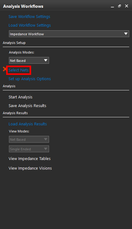
Step 4: Click Select Nets.
Note: This will bring up the XNet Selection dialog box. Here you can select specific nets or all the nets in the design.
Step 5: Press the >> button to select all the nets in the design and click OK.
Note: Select Analysis Options to detect and model coplanar traces in the Impedance Analysis Parameters window. By default, this option is not enabled.
Performing Impedance Analysis
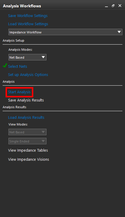
Step 6: Select Start Analysis from the Analysis Workflow Manager.
Note: This will perform the analysis with the progress bar displaying the status of the analysis.
Viewing Impedance Results
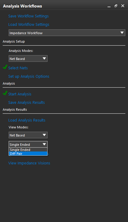
Step 7: Under View Modes select Net Based and Diff Pair (Differential Pairs).
Note: The following Analysis Modes are available to view:
- Net Based: Displays results for all segments or selected nets.
- Directed Group: Displays results for the segments defined in selected directed group. This option is only available if results contain directed group data.
- Single Ended: Displays single ended analysis results for both single-ended and differential pair nets.
- Differential Pairs: Displays differential pair analysis results for differential pair nets and single-ended results for single-ended nets.
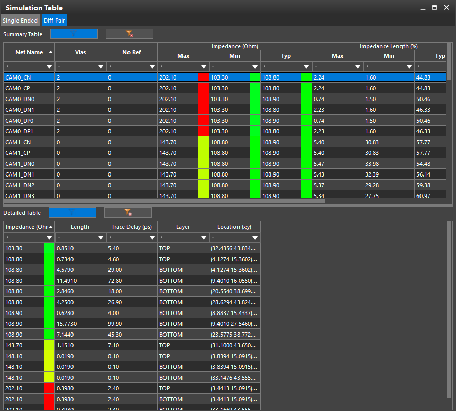
Step 8: Select View Impedance Tables.
Note: The Impedance table is broken down into two different views- the Summary Table and Detailed Table. The Summary Table shows the following information:
- Net Names
- Vias
- No Ref
- Color Coded Impedance Values (Ohm) (Minimum, Maximum, and Typical)
- Impedance Length (%) (Minimum, Maximum, and Typical)
- Trace Total Length
- Trace Total Delay (nS)
The Detailed Table includes the following information:
- Color Coded Impedance (Ohm)
- Length
- Trace Delay (pS)
- Layer
- Location (x;y)
The Single Ended Impedance Table will also show Trace Total R (mOhm), Trace Total L (nH), and Trace Total C (pF).
Step 9: Close the Impedance Table.
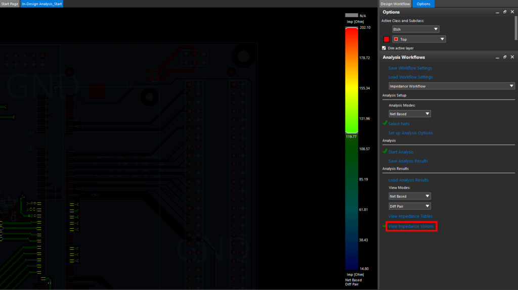
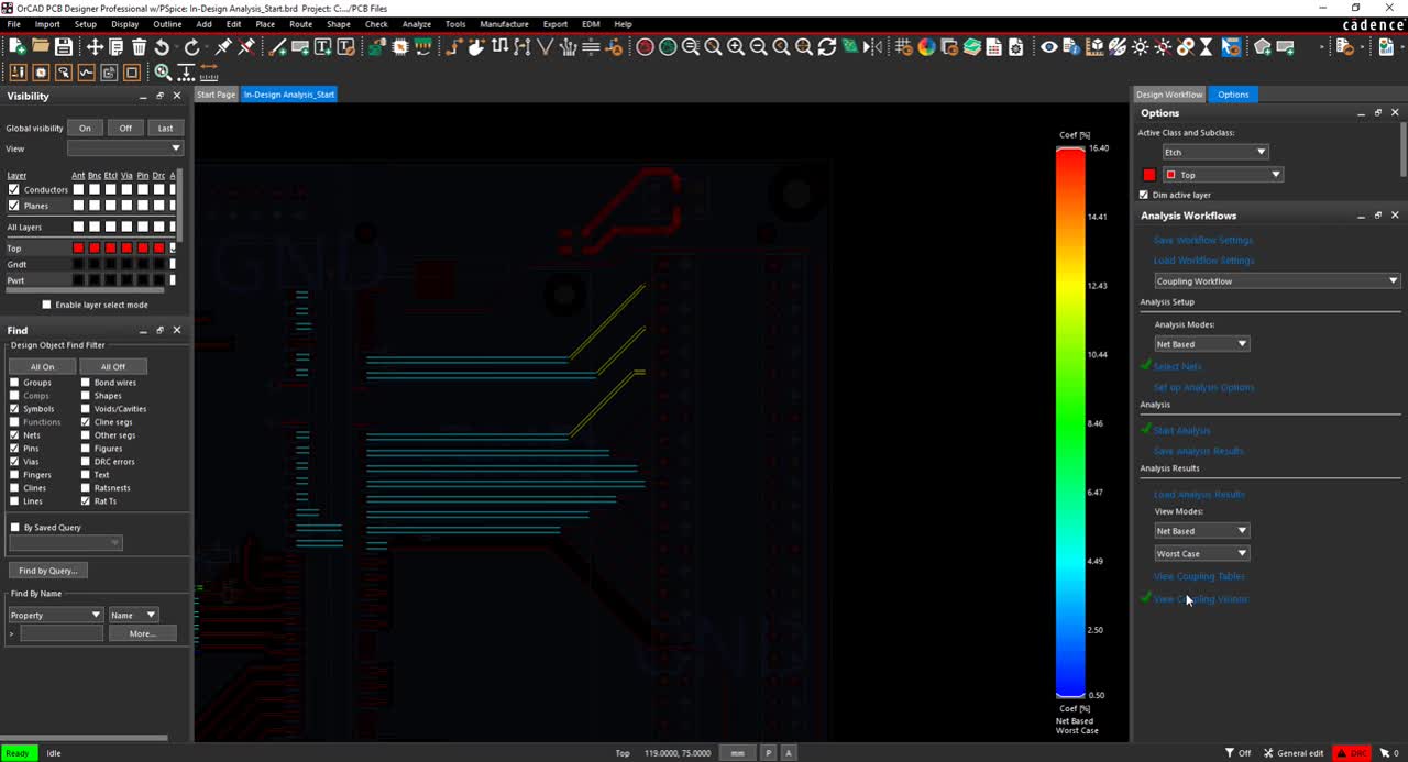
Step 10: Select View Impedance Visions. Adjust the Imp [Ohm] bar to only view traces with problematic impedance values.
Step 11: Select View Impedance Visions again to exit the view.
Configuring Coupling Analysis
Step 12: From the workflow drop-down menu, select the Coupling Workflow.
Step 13: Under Analysis Mode select Net Based.
Step 14: Click Select Nets. Press the >> button to select all the nets in the design and click OK.
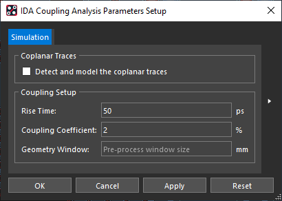
Note: Select Set up Analysis Options to configure Coupling Analysis Parameters including:
- Detect and Model Coplanar traces: Choose to include coplanar data in simulation results. By default, this option is not enabled.
- Coupling (%): Specifies the minimum net level coupling coefficient threshold. The default value is 2%.
- Rise Time (ps): Specifies the rise time for minimum coupled length. The default value is 50 ps.
- GeoWindow: Set a geometry window value in design units for aggressor inclusion for the selected victim nets. All net segments within the specified distance from the selected net, across all layers, will be considered aggressors. This option is only available for coupling analysis and will allow additional potential aggressor traces to be found based on the window.
Performing Coupling Analysis
Step 15: Select Start Analysis from the Analysis Workflow Manager.
Note: This will perform the analysis with the progress bar displaying the status of the analysis.
Viewing Coupling Results
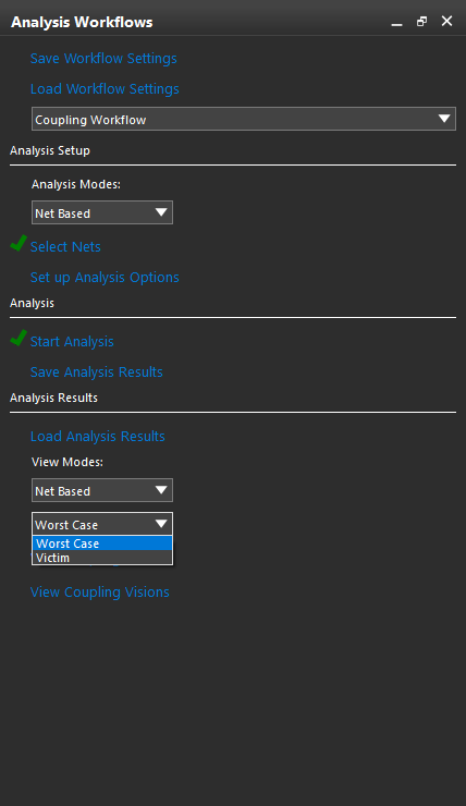
Step 16: Under View Modes select Net Based and Worst Case.
Note: The following Analysis Modes are available to view in the Coupling Analysis:
- Net Based: Displays results for all segments or selected nets.
- Directed Group: Displays results for the segments defined in selected directed group. This option is only available if results contain directed group data.
- Worst Case: Displays the maximum coupling coefficient for all segments or selected nets.
- Victim Analysis: Displays all aggressor segments for a specific victim net.
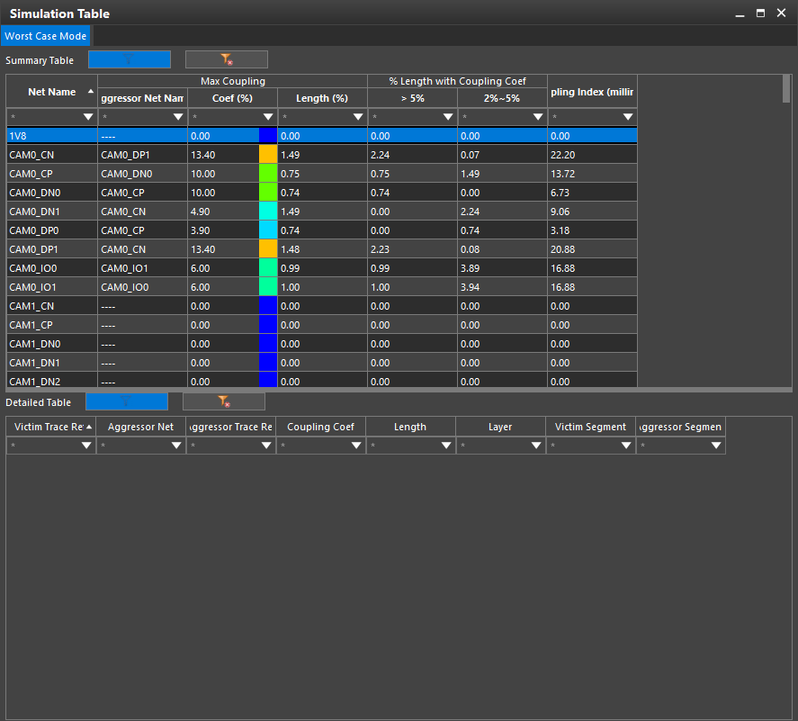
Step 17: Select View Coupling Tables. In the Detailed Table, double-click a net to view the location on the PCB.
Note: The Coupling Table is broken down into two different views- the Summary Table and Detailed Table. The Summary Table shows the following information:
- Net Name
- Max Coupling
- Aggressor Net Name
- Color Coded Coef (%)
- Length (%)
- Percentage of Length with Coupling Coefficient
- >5%
- 2-5%
- Total Coupling Index (millimeter-%)
The Detailed Table includes the following information:
- Victim Trace Ref
- Aggressor Net
- Aggressor Trace Ref
- Coupling Coefficient
- Length
- Layer
- Victim Segment
- Aggressor Segment
Step 18: Close the Coupling Table.
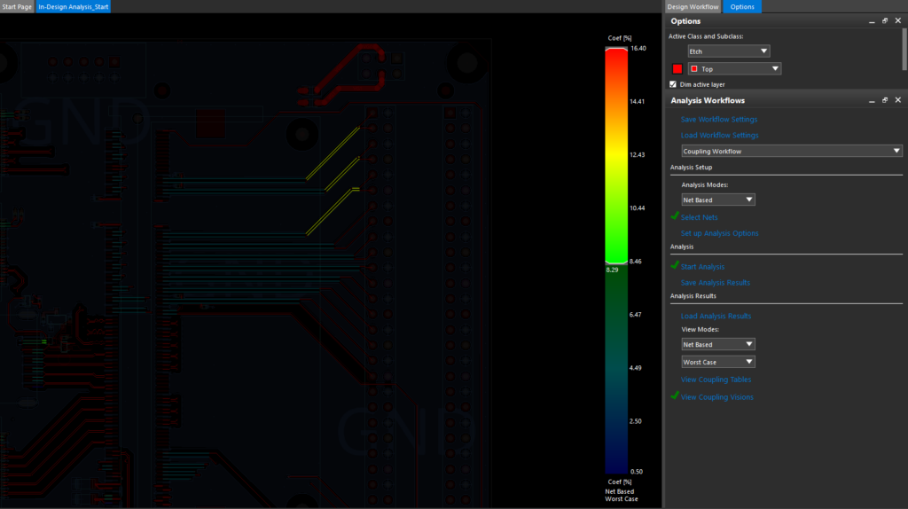
Step 19: Select View Coupling Visions. Adjust the Coef [%] bar to only view traces with problematic coupling coefficient values.
Correcting Coupling Issues
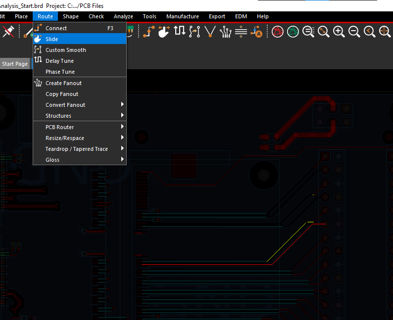
Step 20: Select Route > Slide from the menu and adjust the traces to incorporate additional space between the nets.
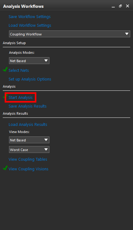
Step 21: Select Start Analysis to see the effect of the PCB modification.
Note: If prompted with the Save Existing Results dialog box, select Ignore to continue with the analysis without saving.
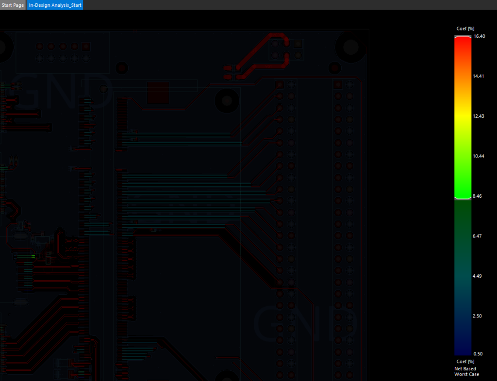
Step 22: View the results. The analysis has completed and the coupling issues have been resolved.
Wrap Up & Next Steps
Quickly analyze critical nets on the PCB, identify potential problems, and improve signal quality during the PCB design with real-time impedance and coupling analysis in OrCAD PCB Designer Professional. For additional signal and power integrity analysis with real-time visual feedback in the PCB canvas, check out Sigrity Aurora to easily analyze return paths, cross-talk, reflection, IR Drop, and more.

