
25.1.4
PCB Editor
Release Date: 06/30/2026
Enhanced Multi-Layer Support for Cut and Undo Cut Operations in Artwork Control Form
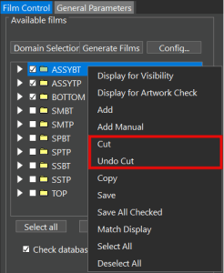 The Cut and Undo Cut options in the Artwork Control Form window can now be used to remove and restore selected item film layers in a single action. When multiple film layers are selected under the Film Control tab, right-clicking any one of them and choosing the Cut option removes all selected layers at once, and selecting the Undo Cut option restores all of them in a single operation.
Performance Improvements
Reuse Saved Queries for Find Filter Selection
Support for Photo Width Text Parameter and OpenType Fonts in GDSII Stream Format
- Allegro X Designer
- Allegro X Designer Plus
- Allegro X Venture
 TI model libraries can be accessed directly from Component Explorer in OrCAD X Capture. Right-click TI-PSpice under Workspace Configuration and choose Show Component Explorer. Requires a valid OrCAD X Cloud subscription.
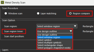 The metal density scan procedure is enhanced to improve density analysis between two regions on the same layer.
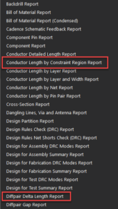 A new quick report has been added and provides conductor lengths within a selected region across all layers. This information helps quickly understand how much routing lies inside or outside a region. It also provides automatic, clear labels indicating how nested or overlapping regions are handled.
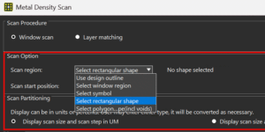 The metal density scan has been enhanced with polygon-based region selection which also supports voids. To improve usability, scan region labels now specify the shape type, rectangular or polygonal, and related option names are clearer.
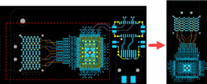 Simplify design reusing by replacing file-based methods and place replicate methods with a direct clipboard-based workflow. You can now copy placement, routing, vias, and shapes between designs without intermediate files, saving time and accelerating design cycles. This method includes intelligent mapping for a seamless transition. Upon pasting, a dialog box guides you through the correct integration of the copied layout into the target design.
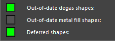 The status command dialog box has been updated with new fields, providing enhanced visibility and control over the status of design shapes. This includes:
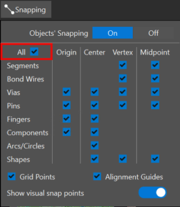 Snapping control has been enhanced and snapping configuration simplified. A new keyboard shortcut has been added to toggle snapping and snapping cursor display without leaving the layout editor, reducing workflow interruptions. A new All check box to activate snapping for all objects has been added, streamlining snapping configuration.
 With this release, OrCAD X Presto introduces the ability to perform instant fanout on multiple pins. Draw a window around a group of pins to select them to perform the instant fanout.
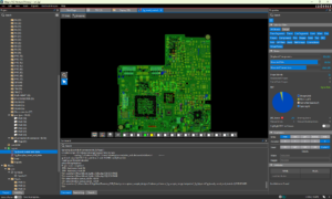 With this unified cockpit designers can seamlessly edit, plan, and modify the PCB layout with the easy-to-use X Layout platform directly in System Capture. This change enhances collaboration between the schematic and PCB layout and incorporates additional features such as preferences and constraints to help communicate design intent upfront.
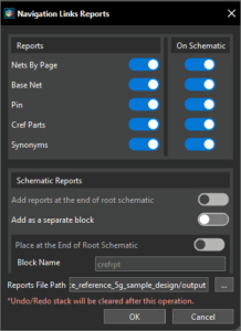 System Capture now supports generating navigation link reports, also called cross-references or CRef reports. Reports for Nets by Page, Base Net, Pin Cross-References, CRef parts, and Synonyms can now be created to be viewed in the schematic or exported as text files. These reports provide detailed connectivity and component cross-referencing insights to help quickly analyze design relationships and locate elements across pages and blocks.
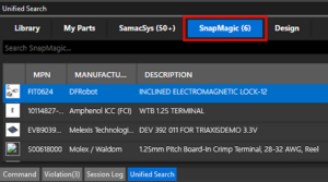 SnapMagic is now available in Unified Search to expand the list of available components. The SnapMagic parts database can be accessed without leaving System Capture.
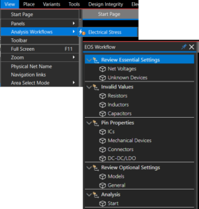 A new workflow to streamline electrical stress analysis has been introduced. The EOS workflow can be accessed under View > Analysis Workflows > Electrical Stress.
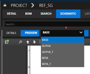 The Pulse web dashboard now supports design variants. To choose a variant, open the Schematic tab and select the Variant dropdown. This enhancement allows designers to switch between variants and easily review or download them.
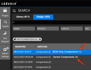 System Capture and the Pulse web dashboard have enhanced design search and version control capabilities. These include:
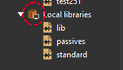 With the new Local Library feature, create and manage libraries directly on your computer. With this new feature, a pulse server connection is not required, all symbols are edited and stored locally with complete formatting support. Anyone can author these local libraries and no role-based restrictions apply. Additionally, custom shapes from managed libraries can be reused and importing pin lists for faster symbol creation is available.
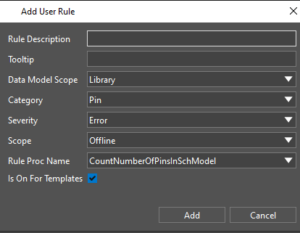 Validation rules now offer enhanced customization for system-defined rules, with the ability to specify the object stages in which they run, such as Validate, Check-in, Pre-Release, and Release. User-defined rules can now be created for all library object types, beyond libraries, parts, symbols, and footprints.
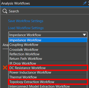 The DC Resistance and Topology Extraction workflows have been added to the IDA workflow list for direct access within System Capture.
 Based on the target IC impedance, estimate and place decoupling capacitors at the schematic stage. A target impedance section is added to the Add Bypass Capacitors and Change Capacitor Quantity windows.
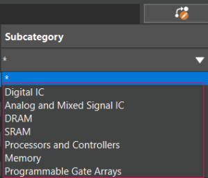 The new subcategories are supported for ICs including Digital IC, Analog and Mixed Signal IC, DRAM, SRAM, Processors and Controllers, Memory, and Programmable Gate Arrays.
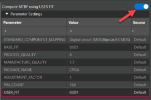 The USER_FIT parameter is now available to calculate MTBF. This parameter is supported for the FIDES standard.
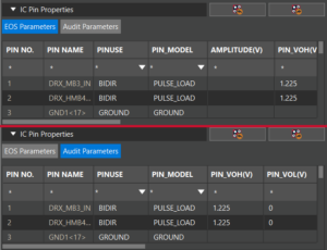 The IC Pin Properties section of the Electrical Stress Settings dialog box now has separate categories for EOS and audit parameters. The EOS parameters now include amplitude (V), pulse width, time period, frequency, and delay.
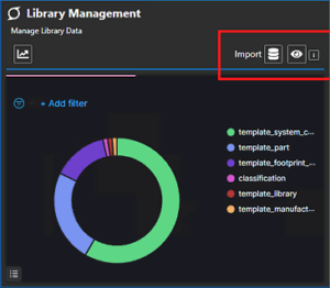 All published data in an Allegro X Managed Library database, including data objects, can be imported into Pulse.