Lesson 10: Design Rule Checks
A Design Rule Check (DRC) checks your design for violations and identifies problem areas with schematic error markers. The DRC report lists all objects checked and the rule violations detected. Schematic Design Rule Checks can be used to identify:
- Unconnected Nets
- Pin Type Conflicts
- Undefined Driving Sources
- Unconnected Pins
- Reference Designator Formatting Errors
This walk-through demonstrates how to view and correct design rule violations in OrCAD X Capture version 25.1. After you complete this topic, you will be able to:
- Configure a design rule check
- Run a design rule check (DRC)
- Identify and correct violations
To follow along, continue with the design from the last topic or use the provided design files. If the design files were not downloaded in the beginning of the Capture Walk-Through, the design files for this lesson can be found under the Materials tab.
 Open in New Window
Configuring a Design Rule Check
Step 1: Select capture_tutorial.dsn in the Project Hierarchy.
Step 2: Select PCB > Design Rules Check from the menu.
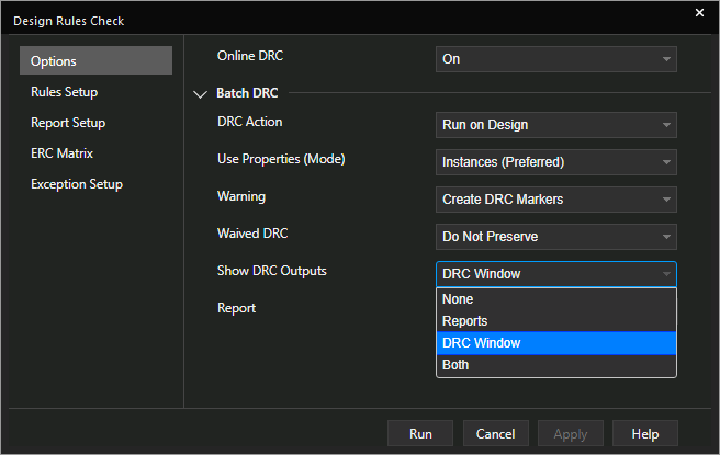
Step 3: In the Options tab, under Batch DRC, select Run on Design from the DRC Action drop-down menu.
Step 4: Select Instances (Preferred) from the Properties (Mode) dropdown.
Note: If you have a hierarchical design, select Occurrences for this setting.
Step 5: Select Create DRC Markers from the Warning dropdown.This will create visual markers on the schematic canvas to indicate errors.
Step 6: Select Do Not Preserve from the Waive DRC dropdown.This will clear any previously-waived DRC errors.
Step 7: Select DRC Window from the Show DRC Outputs dropdown.This will show the error list in the dedicated error panel as opposed to a separate report window.
Step 8: Select the ellipsis for Report to open the file browser.
Step 9: Browse for a location to save the report. Name the report and click Open.
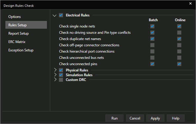
Step 10: Select the Rules Setup tab. Here you can select which electrical and physical rules to check in the design. Custom rules can also be assigned. Leave the default settings.
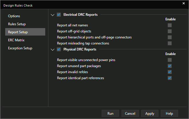
Step 11: Select the Report Setup tab. Here you can select which electrical and physical items are included in the report. Leave the default settings.
Step 12: Select the ERC Matrix tab. This matrix is used to test connections between pins, hierarchical blocks, and hierarchical ports. The ERC Matrix flags invalid pin-to-pin function connections found within the design. The Matrix shows all possible pin-to-pin combinations. Define a pin combination by toggling between valid (empty) or invalid (flagged with an error or warning). Leave the default settings.
Step 13: Select the Exception Setup tab. Here you can define rules you want excluded from the DRC by selecting the Add New button. Leave the default settings.
Running a Design Rule Check
Step 14: Select Run to generate the DRC Report.
Step 15: Click Yes when prompted.
Step 16: When the check finishes, view the markers on the PCB canvas. Each marker indicates a problem area.
Note: You may be prompted to open the DRC report in the system log. Click No.
Analyzing DRC Results
Step 17: Select the DRCs tab at the bottom of the window to open the DRCs panel.
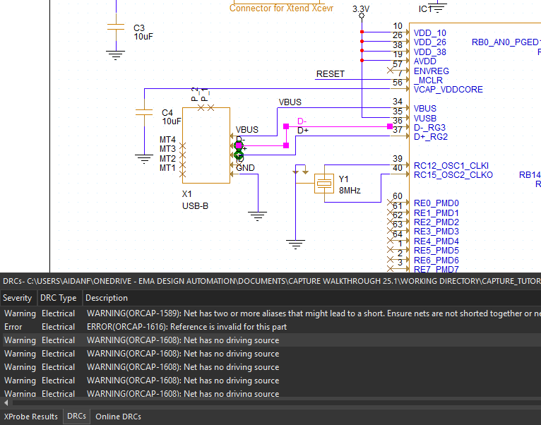
Step 18: Double-click one of the errors to highlight the affected part, net, or pin in the schematic.
Step 19: Correct violations as needed. To waive a DRC, right-click a marker and select Waive DRC.
Step 20: To view the DRC report outside Capture, open File Explorer and browse to the directory where the report was saved. By default, this is the working directory.
Step 21: Open the file in a text editor of your choice, such as Notepad. DRC violations are listed by schematic and type of rule.
Clearing DRC Markers
Note: The errors and warnings listed here are acceptable and can be ignored for this design. The following steps will show how to delete the design rule violation markers on the schematic canvas.
Step 22: Back in Capture, select capture_tutorial.dsn in the Project Hierarchy.
Step 23: Select PCB > Design Rules Check from the menu.
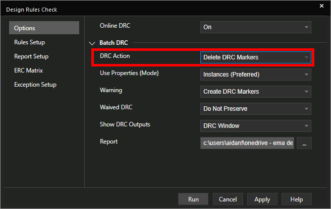
Step 24: In the Options tab, select Delete DRC Markers from the DRC Action dropdown. Click Run.
Step 25: The DRC markers have been removed but the error report remains unchanged.
This completes the lesson on design rule checking in OrCAD X Capture 25.1. In the next lesson, we will discuss how to generate a bill of materials.
