Lesson 13: Netlisting
The netlist communicates the component and connectivity information from the schematic to the PCB layout. This walk-through demonstrates how to generate a netlist and new layout file for your OrCAD X Capture 25.1 schematic. After you complete this topic, you will be able to:
- Create only a netlist
- Create a new PCB layout and netlist in one step
To follow along, continue with the design from the last topic or use the provided design files. If the design files were not downloaded in the beginning of the Capture Walk-Through, the design files for this lesson can be found under the Materials tab.
 Open in New Window
Creating a Netlist
The following steps will create only a netlist. This option can be chosen if you are passing the netlist to a contractor or PCB designer. To create both a PCB Layout and netlist in one step, move ahead to Creating the PCB Layout.
Step 1: Select the capture_tutorial.dsn file in the Project Manager.
Step 2: Select Tools > Create Netlist from the menu. The Create Netlist window opens.
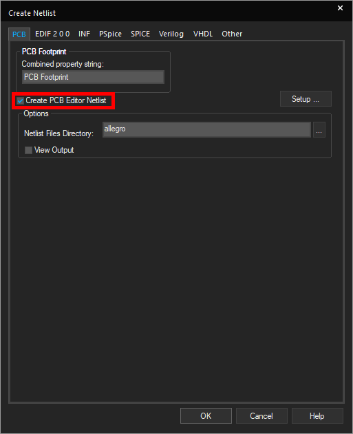
Step 3: Under the PCB tab, check Create PCB Editor Netlist.
Step 4: Under Options, select the ellipsis to browse for a location to save the netlist.
Step 5: The file browser opens. Select the desired folder to save the netlist in and click Select Folder.
Note: Typically, this is a subfolder within the project folder named allegro.
Step 6: If this is your first time netlisting, select Setup.
Step 7: The configuration file needs to be defined. Select the ellipsis.
Step 8: Browse to the location of the allegro.cfg file. The default file path is: C:\Cadence\SPB_25.1\tools\capture.
Step 9: Select the file and click Open. Click OK in the Setup window.
Step 10: Click OK to netlist the design.
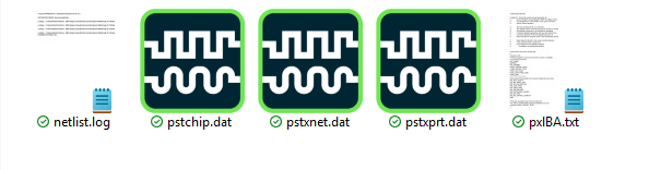
Note: The netlist files pstxnet.dat, pstxprt.dat, and pstchip.dat are generated in the specified location.
Creating the PCB Layout
The following steps will create a PCB layout and automatically netlist the design. This reduces steps and streamlines the PCB Layout process.
Step 11: To configure the PCB layout, select PCB > Design Sync Setup from the menu.
Step 12: The Design Sync Setup window opens. Here you can configure the layout folder, placement options if the board already exists, and more. Select the desired software for the PCB design from the Select Layout Tool dropdown:
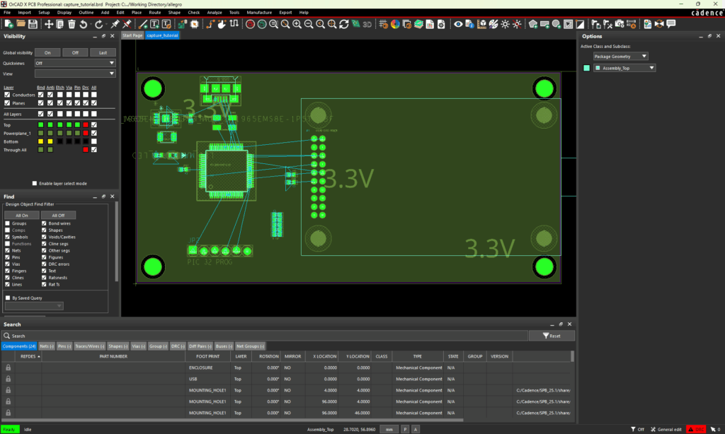
PCB Editor: Classic PCB editing tool
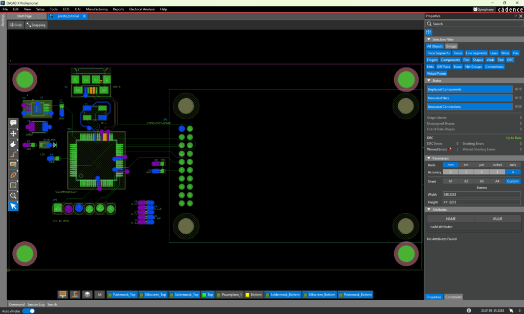
OrCAD X Presto: Newly-released PCB editing environment featuring new UI and improved ease of use.
For this example, we will select OrCAD X Presto. Click OK.
Step 13: To generate the layout, select PCB > New Layout from the menu. The New Layout window opens.
Step 14: Select the ellipses for PCB Layout Folder to open the file browser.
Step 15: Browse for a location for the board file to be saved. Click Select Folder.
Step 16: In the Board field, enter a name for the board file. By default, this is the same as the project name.
Step 17: Leave Input Board File blank to create a new design.
Step 18: Click OK to create the new layout.
Step 19: The Cadence Allegro Product Choices window will open. Select OrCAD X Professional or your required license from the list and click OK. This will open the new PCB layout file, which will be used in the PCB Walk-through.
Next Steps
This concludes the OrCAD X Capture Walk-through. Included in this walk-through are optional bonus lessons to teach you about additional features included in OrCAD X Capture 25.1. These optional lessons include:
- LiveBOM: Real-time supply chain analysis integrated directly into the schematic canvas
- Cloud-based File Management: Share and manage project files directly from OrCAD X Capture including schematics, PCB layouts, libraries, PDFs and more.
- Design Review and Markup: review the schematic, add comments and markup directly in the schematic. Comments and markup are embedded in the design files for efficient communication.
To continue learning with this OrCAD X Walk-through, step through the PCB layout with one of the following walk-through selections:
OrCAD X Presto Walk-Through: New, updated user interface for PCB layout offering streamlined menus, intuitive GUI, and accelerated PCB layout process.
OrCAD X PCB Walk-Through: Classic user interface for PCB Layout
To learn about incorporating SPICE simulation into your schematic design flow, continue learning with the PSpice Walk-through.
