Lesson 7: Part Information
It is critical to define your design intent through schematic and part information such as voltage levels, component values, PCB footprints, and more. This walk-through demonstrates how you can add and edit design part information either before or after part placement in OrCAD X Capture 25.1. After you complete this topic, you will be able to:
- Assign voltage levels
- Edit component values
- Configure the information displayed on the schematic
- Add PCB footprints to your design
To follow along, continue with the design from the last topic or download the provided design under the Materials tab.inning of the Capture Walk-Through, the design files for this lesson can be found under the Materials tab.
 Open in New Window
Assigning Power Net Values
Step 1: Select Edit > Replace from the menu to open the advanced Replace panel. The replace panel is a new feature in OrCAD X Capture 25.1, allowing designers to quickly find and replace information defined in the schematic
Step 2: In the Replace panel, enter VCC into the Objects field. Select Find.
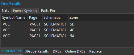
Step 3: The Find Results tab opens automatically. Select Power-Symbols to view the list of fitting symbols. The three VCC power pins are listed.
Note: This table can also list nets and component pins.
Step 4: Select the Replace tab again. Select the plus sign for the Find Properties table to add a property.
Step 5: Select Name from the Property dropdown for the new entry. Enter VCC into the Value field.

Step 6: Select the plus sign for the Replace Properties table. Select Name from the Property dropdown for the new entry and enter 3.3V into the Value field.
Step 7: Click Replace to replace the previously-defined VCC net with 3.3V to connect all power pins to 3.3V. Click Yes for any resulting prompts.
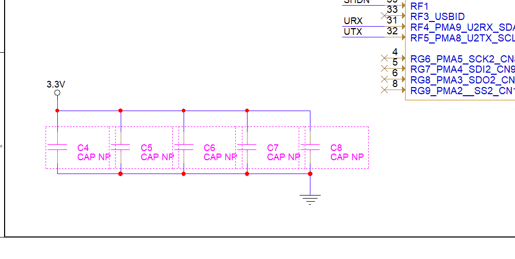
Step 8: View the schematic canvas. All VCC power pins have been replaced with 3.3V pins, connecting to the 3.3V net on the output of voltage regulator U1.
Note: You can also assign voltage values during power pin placement. Select Place > Power from the menu. Select VCC and OK. Before placing, right click and select Edit Properties. Add 3.3V for the value and click OK. Now the component will be placed with the correct value.
Defining Component Values
Step 9: Hold CTRL and click to select the row of parallel capacitors. Right-click and select Edit Properties.
Step 10: The Property Editor tab opens, listing the properties of all selected components. Select the Value row. Right-click and select Edit.
Step 11: Enter a value of 0.1uF and click OK.
Step 12: Close the Property Editor tab. The capacitor values have been updated.
Note: You can also activate the properties window by double clicking a component. You can change the Display Format in the Display Properties window.
Step 13: Hold CTRL and select capacitors C2, C3, and C9. Right-click and select Edit Properties.
Step 14: Select the Value row. Right-click and select Edit.
Step 15: Enter a value of 10uF and click OK. Close the Property Editor tab.
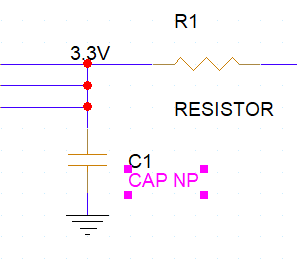
Step 16: Double-click the value (CAP NP) of capacitor C1 to change it.
Step 17: Enter 100uF for the value and click OK.
Note: Easily configure what information is displayed on the schematic in the Display Properties window. The following display format options are available:
- Do Not Display: Do not display the value.
- Value Only: Display the value as entered.
- Name and Value: Display the property name and value.
- Name Only: Display the property name.
- Both if Value Exists: Display the property name and value if the value is defined.
- Value if Value Exists: Display the value if the value is defined.
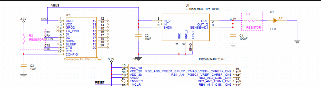
Step 18: Hold CTRL and select resistors R1 and R2. Right-click and select Edit Properties.
Step 19: Double-click the Value cell for R1 and enter a value of 150. Double-click the Value cell for R2 and enter a value of 56k. Close the Property Editor tab.
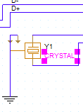
Step 20: Double-click the value, “CRYSTAL”, for crystal Y1.
Step 21: Enter a value of 8MHz and click OK.
Displaying Colors
Step 22: Double-click the value, “LED”, for LED D1.
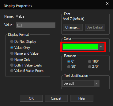
Step 23: Select green from the Color drop-down menu in the Display Properties window.
Step 24: Click OK. The color of the LED value has been changed to green.
Assigning PCB Footprints
Step 25: In the project hierarchy, select PAGE1, right-click and select Edit Object Properties.
Note: This will display the properties for all the components placed on Page 1 of the schematic. Footprints have not been assigned for capacitors, resistors, or the LED. The footprint for the part placed through Ultra Librarian was automatically assigned.
Step 26: Enter 1210 into the cell on the PCB Footprint row under C1 to assign the footprint.
Note: If the footprint name is unknown, open OrCAD X PCB Designer. Select Place > Components Manually from the menu.
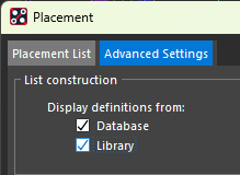
Select the Advanced Settings tab and check Library.
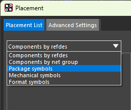
Return to the Placement List tab and select Package Symbols from the drop-down menu.
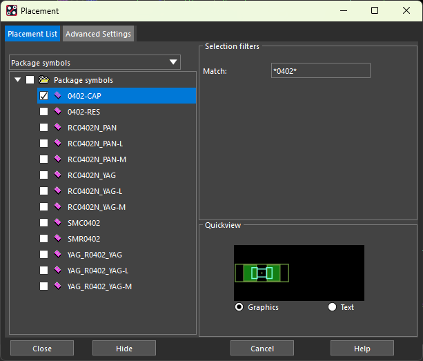
Search for *0402* and press Enter on the keyboard. This will return any footprint with 0402 in the name. Check the box next to the name to preview the 0402-CAP footprint.
Step 27: Enter 0402-CAP into the cell on the PCB Footprint row under C2 to assign the footprint.
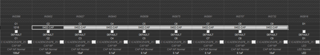
Step 28: Click and drag the marker to extend the footprint to C3-C9.
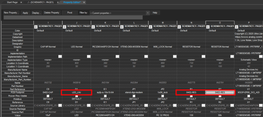
Step 29: Enter LED_LNJ into the cell on the PCB Footprint row under D1 to assign the footprint to the LED.
Step 30: Enter 0402-RES into the cell on the PCB Footprint row under R1 and R2 to assign the footprints.
Note: You can use the keyboard shortcuts CTRL-C and CTRL-V.
Step 31: Click Apply and close the Property Editor tab.
Previewing Footprints in OrCAD X Capture
Step 32: Back in the schematic, right-click a component and select Show Footprint.
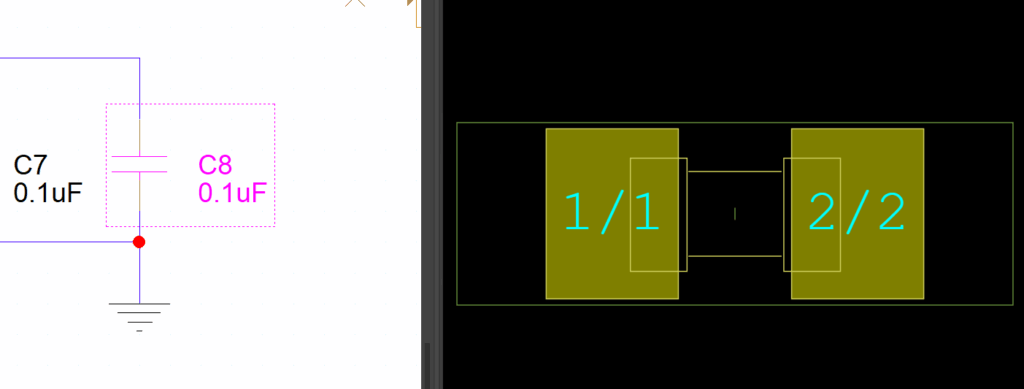
Step 33: Verify the footprint in the Footprint Viewer.
This completes the lesson on adding part information. In the next lesson, you will learn more about part references and multiple methods for annotating the schematic.
