PCB Walk-through 5: Copper Pours
This walk-through demonstrates how create copper pours. After you complete this topic, you will be able to:
- Add ground and power planes
- Draw and merge geometric shapes
To follow along, continue working with the design completed in PCB Walkthrough 4 or open the provided board file in the folder directory, PCB Walkthrough 5_Copper Pours.
 Open in New Window
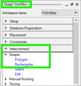
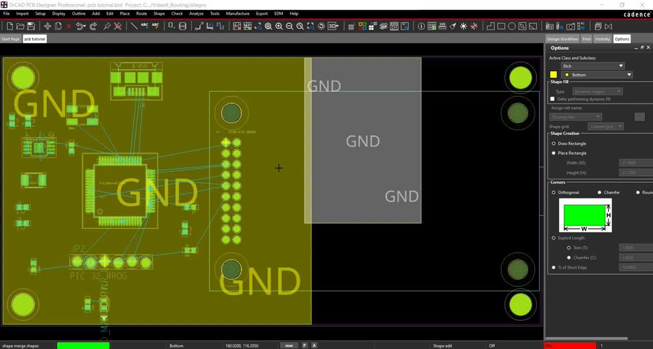
- In the Design Workflow, select Interconnect > Shape > Rectangular.
- In the Options tab, select Etch and Bottom for Active Class and Subclass.
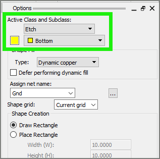
- In Assign Net Name, select GND from the drop-down list.
- Click to draw the rectangle on half of the board.
- Click to draw an overlapping rectangle.
- Right click and select Done.
- Select Setup > Application Mode > Shape Edit from the menu.
- Right click on a shape and select Merge Shapes.
- Click on the other rectangular shape.
- In the Design Workflow, select Interconnect > Shapes > Polygon.
- In the Options tab, assign the net as GND.
- Click and draw your polygon to cover the remainder of the PCB.
- Right click and select Done.
- Right click on the polygon and select Merge Shapes.
- Select the rectangular shape.
Note: OrCAD PCB has dynamic healing for copper pours. You can move your components and mechanical symbols and the copper will heal itself.
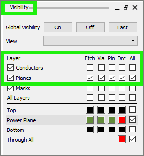
- In the Visibility tab, select the All check box for Conductor to turn off visibility.
- Select Edit > Split Plane from the menu.
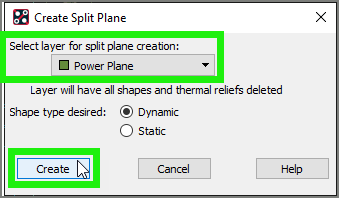
- Select Powerplane_1 as the layer and select Create.
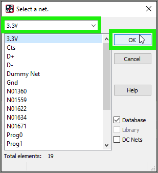
- Assign 3.3V as the net and click OK.