PCB DesignExplore our scalable PCB design solutions designed to growth with your business.
Best price and functionality mix for front to back PCB design.
Enterprise PCB solutions for maximum performance and throughput.
AI Assisted PCB Design to dramatically increase designer productivity & efficiency
Instant access to your own PCB design and library data management environment from anywhere in the world.
Simulation & AnalysisTest and optimize before you build with our array of best-in-class simulation and virtual prototyping solutions.
The gold standard in SPICE circuit design & reliability analysis.
Complete electrical analysis platform built to help you solve all your SI, PI, and EMC design challenges across the board.
RF / Microwave design and verification platform.
Graphical static timing analysis & documentation environment.
Libraries & DataManage your design data with ease and provide actionable insights to prevent problems and reduce time to market with our integrated data management solutions. Learn More
CIP provides library and supply chain intelligence for PCB design teams.
EDM provides design data management, collaboration, and traceability.
Multi-CAD Library Creation & Verification
Enterprise Multi-CAD PDM for advanced PCB design teams.
Cable & Wire HarnessCreate, manage, and document your cable and wire harness assemblies in a comprehensive, integrated platform.
Integrated 2D/3D purpose-built cable & wire harness design platform
3D CAD for enterprise needs and workflows
Computation Fluid Dynamics (CFD) AnalysisGet accurate, on-time CFD analysis results with our advanced simulation and meshing engines. Learn More
Easy-to-use CFD engines optimized for electronics cooling analysis.
Next-gen System level CFD analysis platform built to scale with your needs.
Industry leading multi-CAD mesh generation software.
IC & Package DesignConnected package and IC design solutions built to handle modern 3D-IC and chiplet challenges.
Leading package and chiplet integration platform.
EMA ServicesOur deep domain expertise and 30 years of experience is here to help you with your custom design needs and integration requirements.
Connect and streamline your systems for a complete digital thread of your design.
Build unique capabilities and flows directly into your CAD design tools.
Let us take the burden of library creation off you with library creation services that scale.
Augment your team with the expertise of our PCB design experts to help get your projects completed on-time and on-budget.
EMA Academy
Never stop learning. Leverage our extensive 30+ year of industry experience to help you take your skills to the next level. Visit EMA Academy
Get trained by the experts live with our virtual or in-person course options.
Quick step-by-step guides on popular design topics updated weekly.
Access to the software, and resources you for your education programs.
EMA Resource CenterAccess the resources you need to maximize your design productivity and stay up to date on the latest design trends. Visit Resource Center
Get additional benefits from EMA including free training, apps, and more.
Explore our network of partners and integrations to help support your design needs at all phases
See how you can connect your design tools into your overall processes and flows.
Connect with our list of design service partners.
Connect with us through our regularly scheduled virtual and live events.
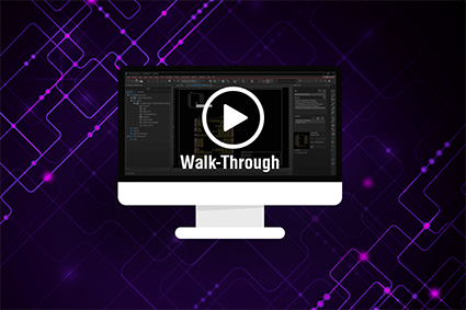
This walk-through will guide you through the process of turning a schematic into a PCB layout using OrCAD PCB Designer 17.4.
The OrCAD PCB 17.4 Walk-Through will guide you through the process of turning your schematic design into a PCB layout using OrCAD PCB Designer.
Don’t have OrCAD? Get your free trial here.
This course is available for these other software versions
Username or Email Address
Password
Remember Me
Username
Email
First Name
Last Name
Country Select CountryUnited StatesCanadaMexicoAfghanistanAlbaniaAlgeriaAmerican SamoaAndorraAngolaAnguillaAntarcticaAntigua and BarbudaArgentinaArmeniaArubaAustraliaAustriaAzerbaijanBahamas (the)BahrainBangladeshBarbadosBelarusBelgiumBelizeBeninBermudaBhutanBolivia (Plurinational State of)Bonaire, Sint Eustatius and SabaBosnia and HerzegovinaBotswanaBouvet IslandBrazilBritish Indian Ocean Territory (the)Brunei DarussalamBulgariaBurkina FasoBurundiCabo VerdeCambodiaCameroonCayman Islands (the)Central African Republic (the)ChadChileChinaChristmas IslandCocos (Keeling) Islands (the)ColombiaComoros (the)Congo (the Democratic Republic of the)Congo (the)Cook Islands (the)Costa RicaCroatiaCubaCuraçaoCyprusCzechiaCôte d'IvoireDenmarkDjiboutiDominicaDominican Republic (the)EcuadorEgyptEl SalvadorEquatorial GuineaEritreaEstoniaEswatiniEthiopiaFalkland Islands (the) [Malvinas]Faroe Islands (the)FijiFinlandFranceFrench GuianaFrench PolynesiaFrench Southern Territories (the)GabonGambia (the)GeorgiaGermanyGhanaGibraltarGreeceGreenlandGrenadaGuadeloupeGuamGuatemalaGuernseyGuineaGuinea-BissauGuyanaHaitiHeard Island and McDonald IslandsHoly See (the)HondurasHong KongHungaryIcelandIndiaIndonesiaIran (Islamic Republic of)IraqIrelandIsle of ManIsraelItalyJamaicaJapanJerseyJordanKazakhstanKenyaKiribatiKorea (the Democratic People's Republic of)Korea (the Republic of)KuwaitKyrgyzstanLao People's Democratic Republic (the)LatviaLebanonLesothoLiberiaLibyaLiechtensteinLithuaniaLuxembourgMacaoMadagascarMalawiMalaysiaMaldivesMaliMaltaMarshall Islands (the)MartiniqueMauritaniaMauritiusMayotteMicronesia (Federated States of)Moldova (the Republic of)MonacoMongoliaMontenegroMontserratMoroccoMozambiqueMyanmarNamibiaNauruNepalNetherlands (the)New CaledoniaNew ZealandNicaraguaNiger (the)NigeriaNiueNorfolk IslandNorthern Mariana Islands (the)NorwayOmanPakistanPalauPalestine, State ofPanamaPapua New GuineaParaguayPeruPhilippines (the)PitcairnPolandPortugalPuerto RicoQatarRepublic of North MacedoniaRomaniaRussian Federation (the)RwandaRéunionSaint BarthélemySaint Helena, Ascension and Tristan da CunhaSaint Kitts and NevisSaint LuciaSaint Martin (French part)Saint Pierre and MiquelonSaint Vincent and the GrenadinesSamoaSan MarinoSao Tome and PrincipeSaudi ArabiaSenegalSerbiaSeychellesSierra LeoneSingaporeSint Maarten (Dutch part)SlovakiaSloveniaSolomon IslandsSomaliaSouth AfricaSouth Georgia and the South Sandwich IslandsSouth SudanSpainSri LankaSudan (the)SurinameSvalbard and Jan MayenSwedenSwitzerlandSyrian Arab RepublicTaiwan (Province of China)TajikistanTanzania, United Republic ofThailandTimor-LesteTogoTokelauTongaTrinidad and TobagoTunisiaTurkeyTurkmenistanTurks and Caicos Islands (the)TuvaluUgandaUkraineUnited Arab Emirates (the)United Kingdom of Great Britain and Northern Ireland (the)United States Minor Outlying Islands (the)UruguayUzbekistanVanuatuVenezuela (Bolivarian Republic of)Viet NamVirgin Islands (British)Virgin Islands (U.S.)Wallis and FutunaWestern SaharaYemenZambiaZimbabweÅland Islands
Registration confirmation will be emailed to you.