PCB Walk-through: Getting Started
This walk-through will assist in setting up the downloaded design files, allowing you to follow along with the PCB Walk-through video series.
 Open in New Window
- Download the zipped practice files under the ‘materials’ tab.
- Save the file to your computer and open.
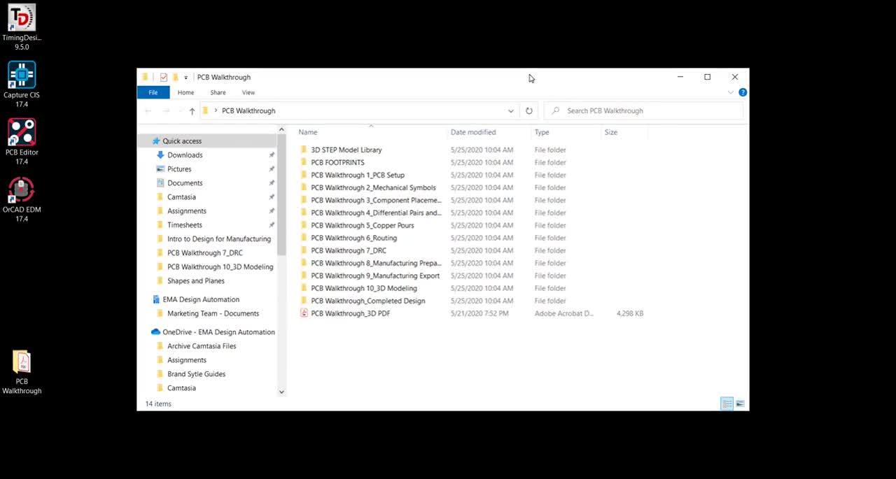
Note: Included in the zipped file is a 3D STEP Model Library, a PCB Footprint library, starting design files for every video, a completed design file, and a 3D PDF of the completed design.
- Open the PCB Footprints folder.
- Select All contents in the folder and Copy (CTRL+C).
- Paste (CTRL+V) the files into the standard OrCAD PCB Footprint and Padstacks library location:
C:\Cadence\SPB_17.4\share\pcb\pcb_lib\symbols
Note: If you followed along with the Capture Walk-through video series this step does not need to be completed again.
- Open the 3D Step Model Library folder.
- Select All contents in the folder and Copy (CTRL+C).
- Paste (CTRL+V) the files into the standard 3D Model library folder using the path below:
C:\Cadence\SPB_17.4\share\local\pcb\step