PCB Walk-through 1: PCB Setup
This walk-through demonstrates how to setup the board configuration. After you complete this topic, you will be able to:
- Setup and edit design parameters
- Add a layer to the board stack up
To follow along, open the provided PCB TUTORIAL.brd file in the folder directory, PCB Walkthrough 1: PCB Setup.
 Open in New Window
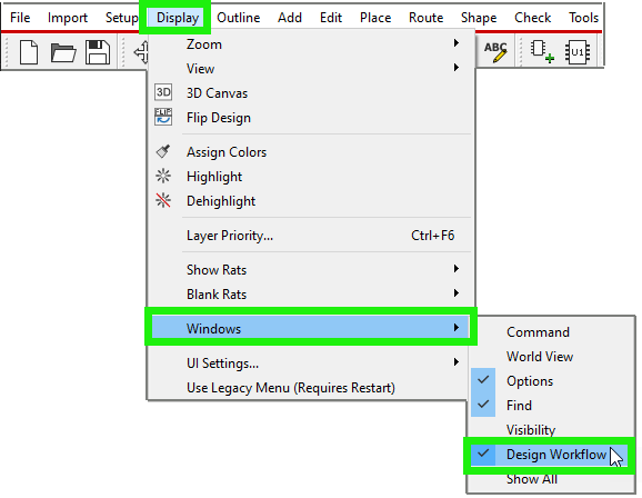
- Select Display > Windows > Design Workflow from the menu.
- In the Design Workflow, select Setup > Design Parameters.
Note: In the Design Parameter window, you can specify parameters for display, design, text, shapes, routing, and manufacturing.
- Select the Design tab.
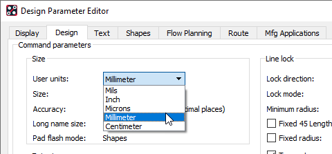
- Set the User Units to Millimeter.
- Click OK.
- In the Design Workflow, select Grids.
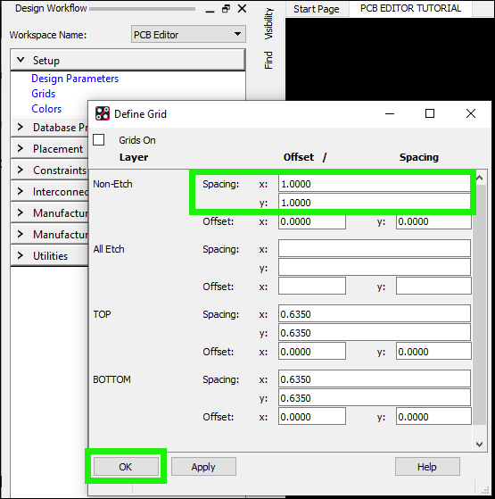
- For Non-Etch, set the Spacing to 1 for both X and Y input fields.
- Click OK.
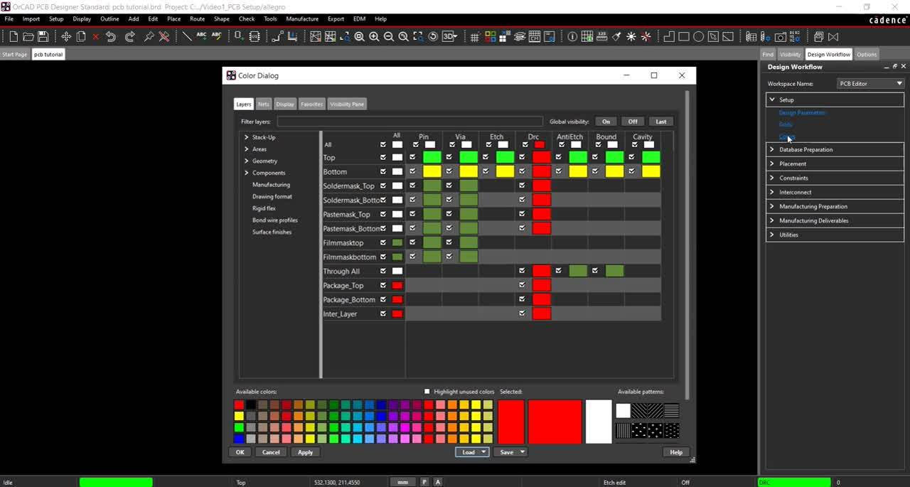
- In the Design Workflow, select Colors.
Note: Here you can specify colors in the design for layers, nets and more.
- Leave the default settings and close the window.
- In the Design Workflow, expand Database Preparation.
- Select Board Outline > Create > Automatically.
Note: Make sure Create is checked in the Design Outline window.
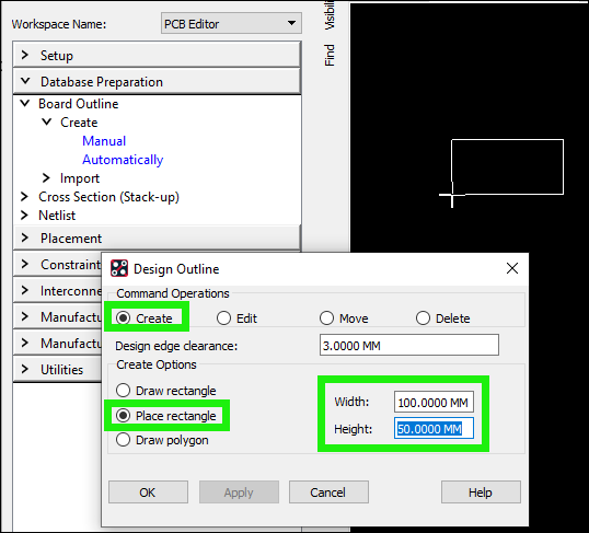
- Enter 0.3 MM for the Design Edge Clearance.
- Select Place Rectangle.
- Enter 100 MM for the Width.
- Enter 50 MM for the Height.
- Click the design canvas to place the board outline.
- Click OK.
- In the Design Workflow, select Cross Section (Stack-up) > Create.
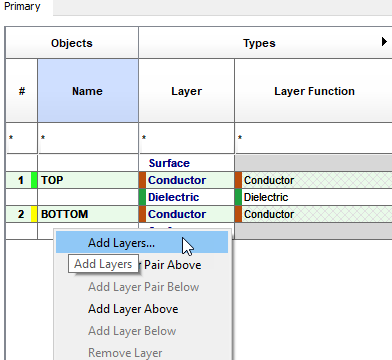
- Right Click in the name column and Select Add Layers.
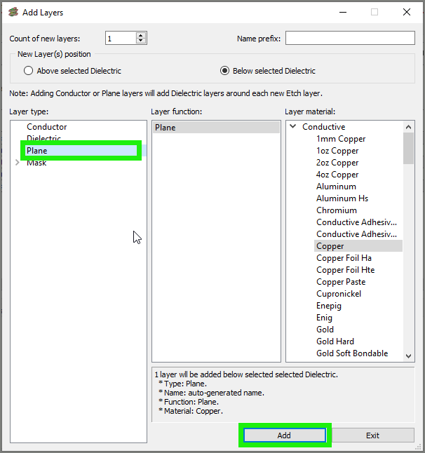
- Assign POWERPLANE as the Name Prefix.
- Select Below selected Dielectric as the New Layer Position.
- For Layer Type, select Plane.
- Click Add and Exit.
Note: This has added the plane and dielectric layer.
- Click OK to close out of the cross-section window.
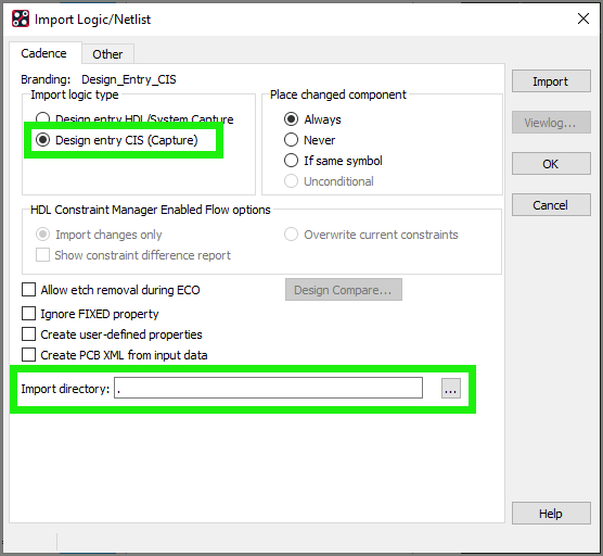
Note: If you need to import a netlist, select Netlist > Import in the Design Workflow. Select Design Entry CIS and set the import directory as the folder location of your netlist. Click Import.
