PCB Walk-through 3: Component Placement
This walk-through demonstrates several different options for placing components on your PCB. After you complete this topic, you will be able to:
- Place components
- Review a report that identifies unplaced components
- Cross probe components between Capture and PCB Editor
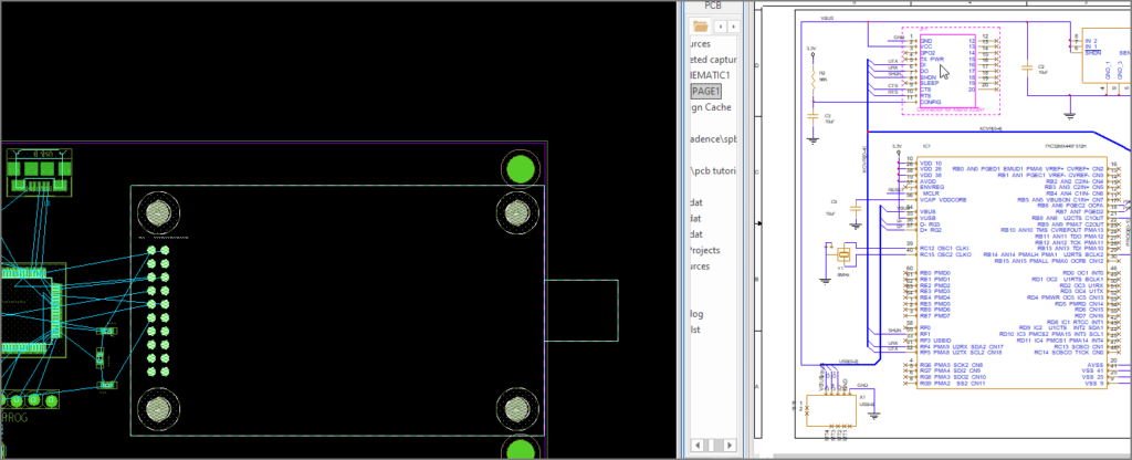
To follow along, continue working with the design completed in PCB Walkthrough 2 or open the provided board file in the folder directory, PCB Walkthrough 3_Component Placement.
 Open in New Window
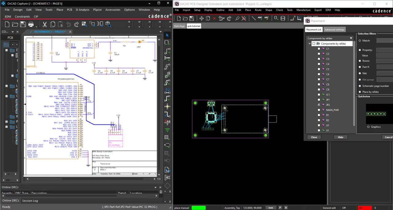
- Open the provided Complete Capture Tutorial.dsn file in OrCAD Capture and the pcb tutorial.brd in OrCAD PCB Designer Professional. Set up a split screen configuration.
- In OrCAD Capture, select Options > Preferences from the menu.
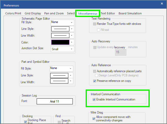
- In the Miscellaneous tab, check Enable Intertool Communication. Click OK.
- In OrCAD PCB Designer, select Placement > Manual from the Design Workflow.
- In OrCAD Capture, select IC1.
- Move the mouse to OrCAD PCB Designer.
- Click to place the footprint.
- Complete this process for the placement of JP1, JP2, and X1.
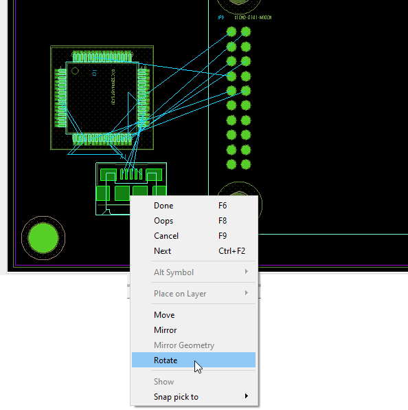
Note: To rotate a part during placement, right click and select Rotate.
- In OrCAD PCB Designer, close the placement window.
- In the Design Workflow, select Placement > Manual.
Note: The already placed components have been removed from the list.
- In the Placement window, select the box next to Components by refdes.
Note: This will select all the components left to place.
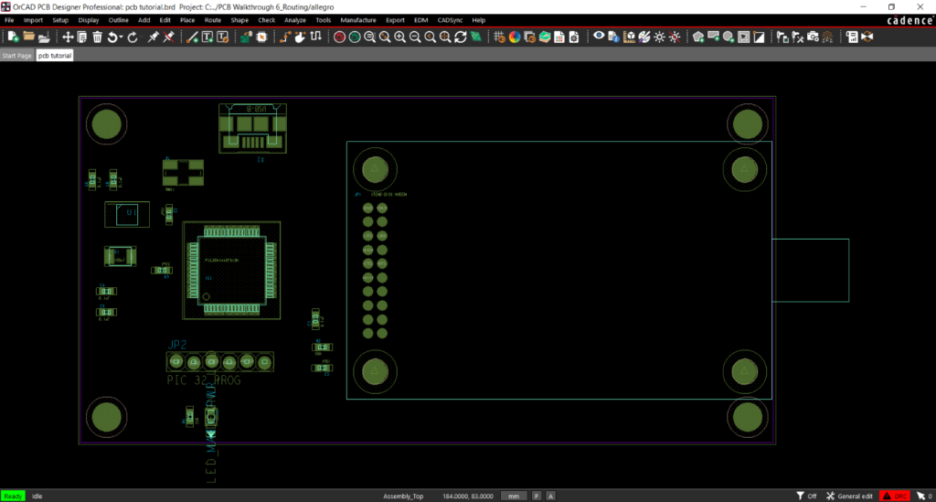
- Click place the remaining components.
- Close the Placement Window when finished.
- In the Design Workflow, select Placement > Report.
Note: This will report any unplaced components. If any components need to be moved, select Setup > Application Mode > Placement Edit from the menu. Click a component and click to place.
- In OrCAD Capture, select a component to cross-probe.
Note: The selected component is shown in OrCAD PCB Designer.
