PCB Walk-through 4: Constraints
This walk-through demonstrates how to set up differential pairs and constraints using OrCAD PCB Designer Professional. After you complete this topic, you will be able to:
- Set up a differential pair
- Specify electrical, physical and differential pair rules with Constraint Sets
To follow along, continue working with the design completed in PCB Walkthrough 3 or open the provided board file in the folder directory, PCB Walkthrough 4_Constraints.
 Open in New Window
Note: If you did not define your differential pairs at the schematic level, use the following steps for definition in the PCB:
- Select Setup > Add Differential Pairs from the menu.
- Select Auto Generate.
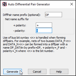
- Assign DP_ for the name.
- Set the + polarity to +.
- Set the – polarity to –.
- Click Generate.
- Click OK to close the window.
This has generated the differential pair.
- In the Design Workflow, select Constraints > Modes.
Note: In the Modes window, select which constraints will be checked by setting the constraints “On” or “Off”. Electrical constraints are available in OrCAD PCB Designer Professional.
- Close the Mode window.
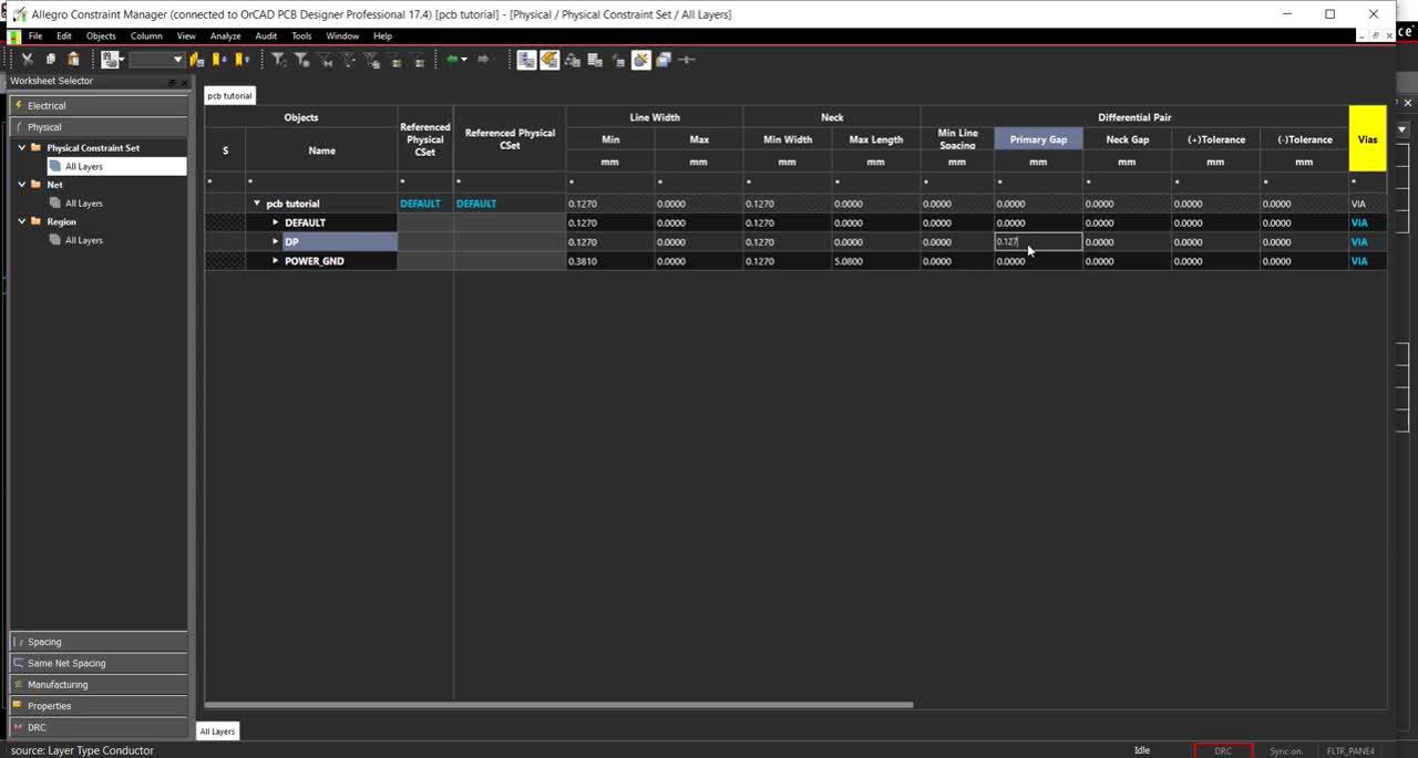
- In the Design Workflow, select Constraints > Physical.
Note: This opens the constraint manager window. In the constraint manager, you can assign electrical, physical, and spacing constraints. Assign constraints by creating Csets or assigning values to each individual net.
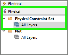
- In the constraint manager window, select the Physical Constraint Set > All Layers.
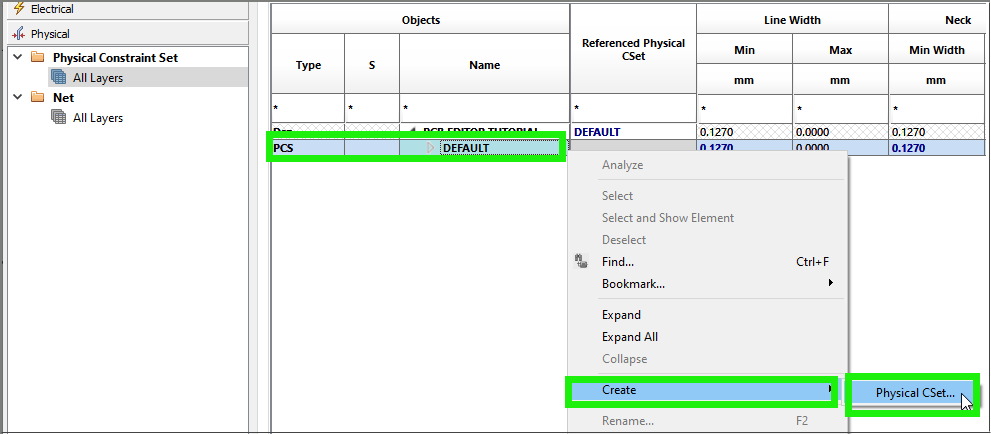
- Right click and select Create > Physical CSet.
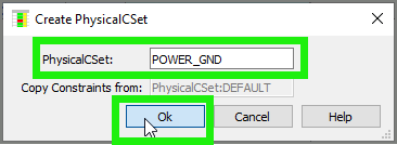
- Name the constraint set POWER_GND and click OK.
- Set the following constraint values:
- Minimum line width: 0.381
- Minimum neck width: 0.127
- Maximum neck length: 5.08
- Right click and select Create> Physical CSet.
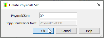
- Name the constraint set DP and click OK.
- Set the following constraint values:
- Line Width: 0.127
- Primary Gap: 0.127
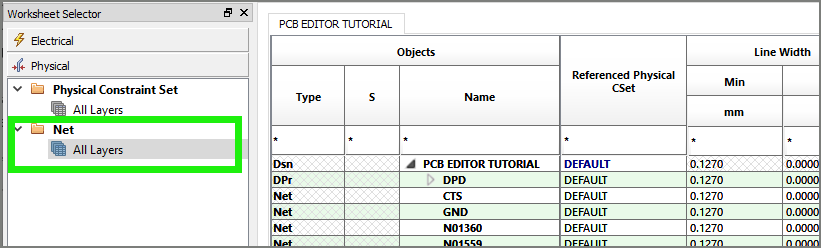
- In the worksheet selector, select Net > All Layers.
- In the Referenced Physical CSet column, assign the POWER_GND CSet to 3.3V and GND.
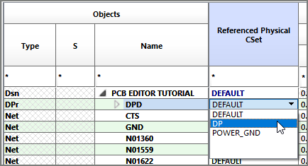
- In the Referenced Physical CSet column, assign the DP CSet to DPD.
Note: Assign the differential pair Cset (DP) at the top level to apply to each net.
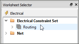
- In the worksheet selector, select Electrical > Electrical Constraint Set > Routing.
- Right click and select Create > Electrical CSet.
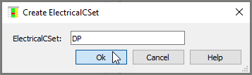
- Name the CSet DP and click OK.
- Set the following constraint values:
- Gather Control: Ignore
- Uncoupled Length: 5.08
- Static Phase Tolerance: 0.508
- In the Worksheet Selector, select Net > Routing > Differential Pair.
- In the Referenced Electrical CSet column, assign the DP Cset to DPD.
- In the Worksheet Selector, select Properties > Net > General Properties.
- Assign 0 to GND.
- Assign 3.3 to 3.3V.
- Close the Constraint Manager Window.
