In complex, high-density designs, performing pin swapping on connectors and programmable components is necessary to optimize routing, improve the stackup, and reduce the number of required vias. However, this can be a daunting task which needs to be completed and verified in both the PCB Layout and the schematic to ensure design accuracy. SKILL can be used to script this process, automatically determining the optimal pin assignments and swapping the pins accordingly.
This how-to will provide step-by-step instructions on how to use the Pin Swapping script written by Robert Finley, to optimize the PCB layout through automatic pin swapping on connectors and programmable devices. To follow along, download the demo files above the table of contents.
How-To Video

Preparing a Design for Pin Swapping
Step 1: Open the provided design, swapback_example.DSN, in OrCAD Capture.
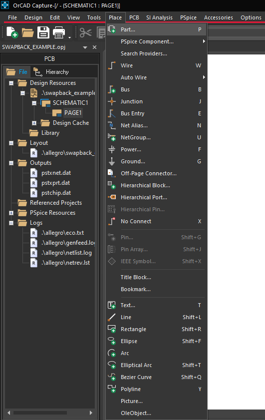
Step 2: Select Place > Part from the menu.
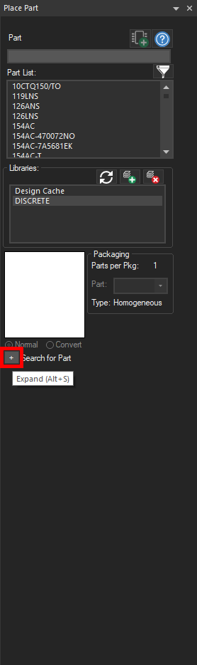
Step 3: Expand the Search for Part sub-pane by selecting the + to the left of Search for Part.
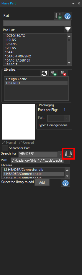
Step 4: Enter *HEADER* into the search bar and click the Part Search button or press Enter on the keyboard.
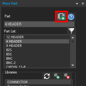
Step 5: Select the part labeled 4 HEADER/Connector.olb and click Add.
Note: The CONNECTOR library has been added to the library list and the 4 HEADER component has been automatically selected.
Step 6: Select the Place Part icon.
Step 7: Click the schematic canvas to place the part.
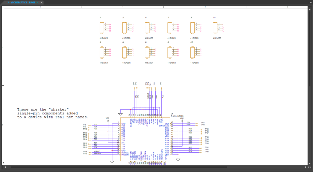
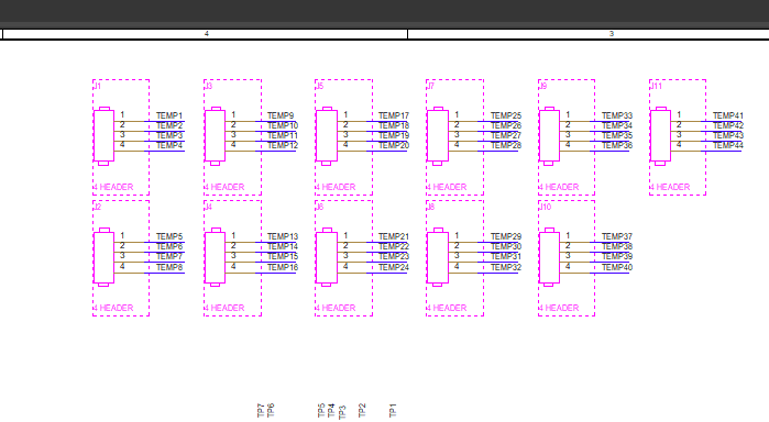
Step 8: Place a total of eleven instances of the header. When finished, right-click and select End Mode (ESC).
Note: These headers will act as routing guides. If headers are not automatically annotated during placement, this can be configured by selecting Options > Preferences > Miscellaneous > Auto Reference > Automatically reference placed parts.
Step 9: Select Place > Wire from the menu, the Wire button on the toolbar, or press W on the keyboard.
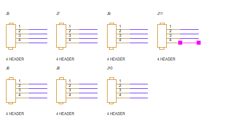
Step 10: Click to place a short wire on each pin of each header. When finished, press Escape on the keyboard.
Note: To quickly duplicate the previously placed wire, press F4 on the keyboard. Using this command, a wire will be placed under the previous wire at the next grid spacing.
Step 11: Select Place > Net Alias from the menu, the Net Alias button on the toolbar, or press N on the keyboard.
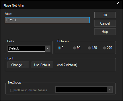
Step 12: Enter TEMP1 as the net alias. Click OK.
Step 13: Click to place the alias on each net. The number will increment automatically as each alias is placed. When finished, right-click and select End Mode or press Escape on the keyboard.
Assigning PCB Footprints
Step 14: Right-click and select Selection Filter or press CTRL-I on the keyboard. The Selection Filter window will open.
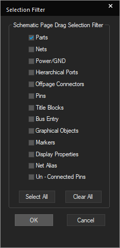
Step 15: Select Clear All to deselect all checkboxes then check the box for Parts. Click OK.
Step 16: Drag a box over all headers to select them.
Step 17: Right-click and select Edit Properties. This will open the Property Editor tab.
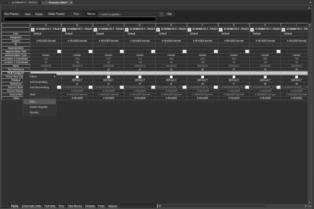
Step 18: Select PCB Footprint from the property column. Right-click and select Edit.
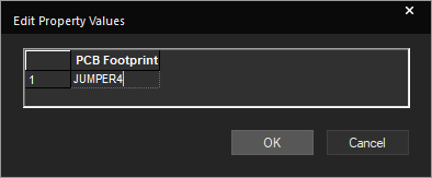
Step 19: Set the footprint name to JUMPER4 and click OK.
Note: The JUMPER4 footprint has been assigned to all headers.
Step 20: Click Apply and close the Property Editor tab.
Updating the PCB Layout
Step 21: Select PCB > Update Layout from the menu.
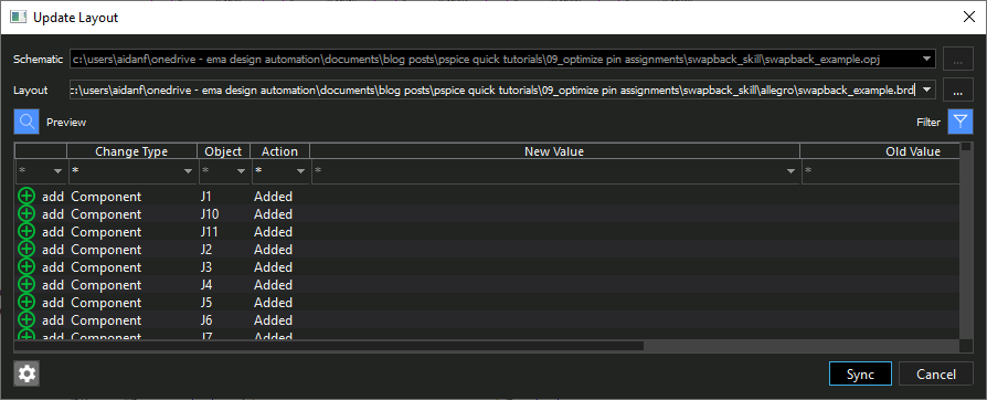
Step 22: The Update Layout window will open. Click Sync.
Note: This will open the PCB layout in OrCAD PCB Designer. A pop-up window may appear to select the desired PCB software.
Placing Components on the PCB
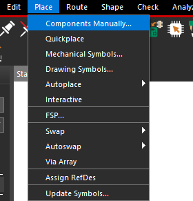
Step 23: Select Place > Components Manually from the menu.
Note: The Placement window will open with a list of components left to place. These are the headers added in preceding steps.
Step 24: Check the box next to Components by Refdes to place all headers at once.
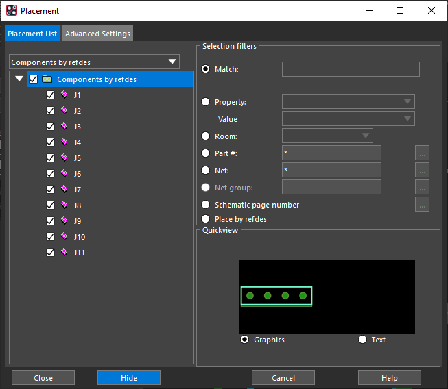
Step 25: Click Hide to hide the Placement window.
Note: Closing the window will prevent placement of any components.
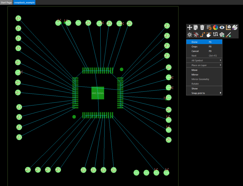
Step 26: Click to place the headers on top of test points. Make sure that each test point is covered by a pad. Right-click and select Done when finished.
Note: This process will intentionally create DRC error markers.
Step 27: Select File > Save from the menu.
Running the SKILL File in OrCAD PCB
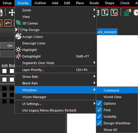
Step 28: Select Display > Windows > Command from the menu to open the Command window.
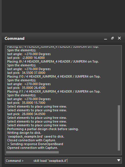
Step 29: Enter the command skill load “swapback.il” into the command window and press Enter on the keyboard.
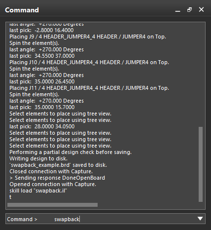
Step 30: PCB Designer will respond with “t.” Type swapback and press Enter to launch the script.
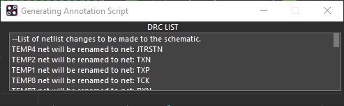
Step 31: The Generating Annotation Script window will open. Scroll to view the list of changes to be made. Close the window.
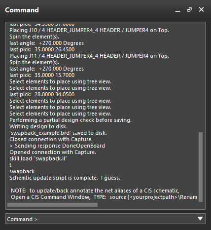
Note: A message will appear in the Command window when the script finishes.
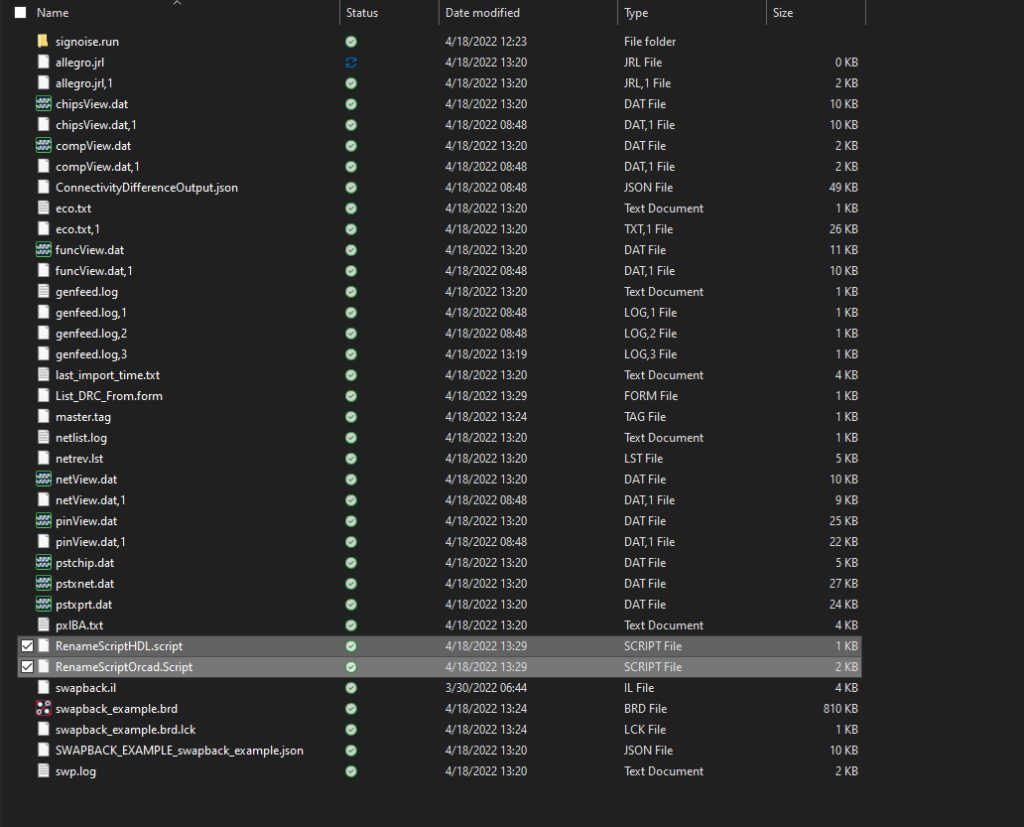
Step 32: Confirm that the generated .Script files exist in the project’s allegro directory.
Running a Script in OrCAD Capture
Step 33: Return to OrCAD Capture.
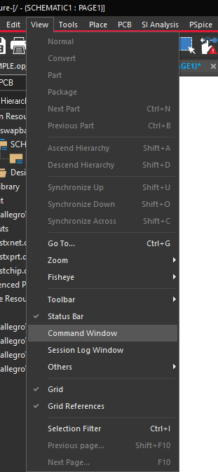
Step 34: Select View > Command Window from the menu.
Step 35: In the command window, place the cursor on the last line.
Note: If the last line does not start with Capture>, press Enter on the keyboard and place the cursor on the appropriate line.
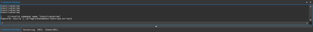
Step 36: Enter the command source {.\allegro\RenameScriptOrcad.Script} and press Enter on the keyboard.
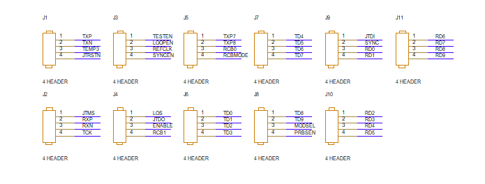
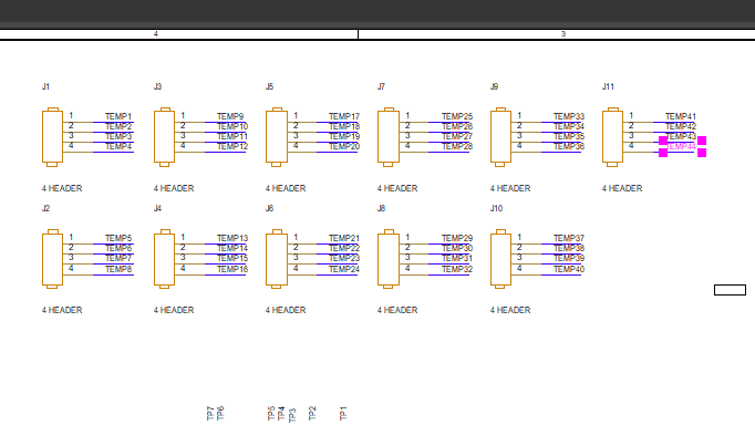
Step 37: View the results. The nets connecting to J1-J11 have been named accordingly.
Wrap up & Next Steps
Quickly perform pin swapping on connectors and programmable components to optimize routing, improve stackups, and reduce the number of required vias with SKILL in OrCAD. See how the features of OrCAD PCB can accelerate your PCB Layout with a free trial.
