Need Help? Get step-by-step instructions for performing HDI Routing in OrCAD X Presto here.
Control Maximum Stacked Via Count
Location: PCB Canvas (Allegro X Venture Only)
If using stacked vias, consider setting Design For Fabrication constraints to control the maximum allowable stacked vias. Access these settings in the constraint manager by selecting Manufacturing > DFF> Holes.
Constraint Regions for Vias
Location: PCB Canvas
Via lists often contain several candidates that would be leveraged during interactive routing; however Allegro X AI will not know when to use special case vias such as testpad or soldermask/metal defined pads. Consider creating constraint regions to define non-default vias; for example, a specific microvia to be used only in a region (micro BGA application).
Need Help? Get step-by-step instructions for creating and managing constraint regions here.
Configure HDI Rules
Location: PCB Canvas
Proper rules need to be configured to ensure the accuracy of HDI routing. For any HDI routing configuration the following rules should be configured:
Any HDI Via Configuration
- Padstack definition
-
- Enable Microvia usage option for all microvias.
- Core via represented as BB via in database.
- Consider non-standard drill attributes (laser in most cases, this impacts NC applications).
- Consider user-defined mask layers (Fill, Plug, etc.).
- Via List
Prioritize the order of vias in each physical constraint set.
Additionally ensure rules are defined accurately based on your HDI configuration including same net spacing, drill hole rules, and physical rules including Pad to Pad connect. “Pad-Pad Connect” defines whether vias are stacked or staggered when Allegro X AI adds the vias.
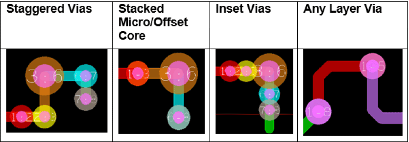
Staggered Vias
- Same Net Spacing Rules
uVia-uVia = 0 or greater
uVia-BB Via = 0 or greater
- Physical Rules
Min/max stagger rule is not necessary unless controlling the maximum distance between vias.
- Drill Hole Rules
Not applicable unless removing pads on core vias or thru pins/vias.
Stacked Micro/Offset Core
- Same Net Spacing Rules
uVia-uVia = 0 or greater
uVia-BB Via = 0 or greater
- Physical Rules
Pad-Pad Connect = Vias_Vias_Only on common layers of the stack.
Minimum BB Stagger = 0
- Drill Hole Rules
Not applicable unless removing pads on core vias or thru pins/vias.
Inset Vias
- Same Net Spacing Rules
uVia-uVia = -1
uVia-BB Via = -1
- Drill Hole Rules
Same Net Hole to Via = 0 or greater for overlap condition.
Any Layer Via
- Physical Rules
Pad-Pad Connect = All allowed
Minimum stagger = 0
Enable Via Labels
Location: PCB Canvas
Via labels will help you visualize the via connections being made. Enable via labels by selection Setup > Design Parameters > Display. Change the label color in the Color Dialog – Display folder for better visibility. The following labels are used for HDI routing:
N:N – Single BB via
N-N – Series of stacked vias
