DFA Package to Package Spacing Constraints
Location: PCB Canvas
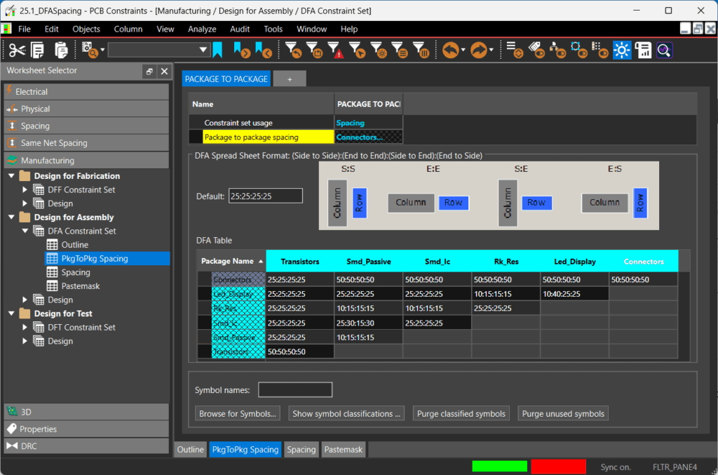
In the constraint manager, define and assign design for assembly constraints detailing the necessary spacing for components based on the configuration of the components (side to side, end to end, side to end, and end to side). This will aid in component placement and ensure components placed by Allegro X AI can be properly assembled based on your manufacturing spacing requirements.
Recommendations:
If your component footprints do not have DFA boundaries, set the Class to Class Spacing in the Allegro X AI panel instead of these DFA Package to Package Spacing Constraints.
Need Help? Get the step-by-step instructions for defining DFA spacing constraints here.
Class to Class Spacing
Location: Allegro X AI
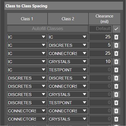
If DFA spacing rules are not configured or if additional spacing is required beyond the constraints configured, assign class to class spacing within Allegro X AI. Users can define the additional spreading requirements beyond the minimum DFA values which can be especially important for the following cases:
- BGAs: Allocate extra clearance from BGAs to other components to support breakout routing
- Testpoints: Define additional clearances to accommodate larger probes during testing
- Connectors: Define additional clearances for assembly and handling
Recommendations:
Run Allegro X AI with no extra clearances then adjust based on results.
Proceed with caution when increasing IC-Discrete clearances as this could degrade decoupling capacitor placement from initial runs (25 mil spacing between ICs and discretes is an acceptable value).
Need Help? Get step-by-step instructions to define class to class spacing rules in Allegro X AI here.
Room Properties
Location: Schematic or PCB Canvas
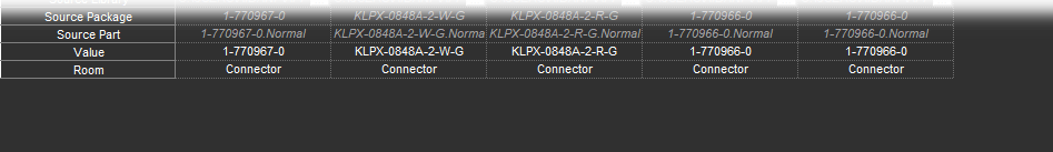
Room properties associate components with an area on the PCB. Components can be assigned to rooms in the schematic or PCB. This will help Allegro X AI cluster components in groups based on functionality and connectivity and impact the quality of results.
Need Help? Get the step-by-step instructions for how to Assign Components to Rooms in the Schematic.
Hard Rooms
Location: PCB Canvas
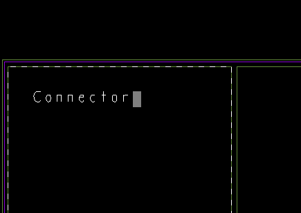
Setting hard rooms is not required but may be useful for locating circuits to desired locations. If physical rooms are drawn on the PCB, these become a “Hard” room where the placement engine confines the respective components within the room boundary and layer usage is fixed as this is derived from the Allegro room setup.
If physical rooms are NOT drawn and only room properties exist, “Floating” rooms will be created where components in a room are clustered, and Allegro X AI will determine a location.
Recommendations:
Only use this hard room option if all parts will fit into the room assignment.
It is recommended that users do NOT over constrain the design.
Only 1-2 fixed rooms for critical circuitry are recommended, if hard rooms are necessary.
Need Help? Get step-by-step instructions for how to create hard rooms in the PCB here.
Room Placement
Location: Allegro X AI
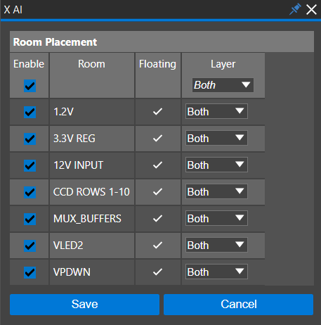
If rooms are configured in the design database, you can select which rooms Allegro X AI should adhere to. Simply enable the rooms you would like Allegro X AI to place. Additionally, define the layer placement of rooms (if not defined by hard rooms on the PCB). This will define if “floating” rooms are placed on the top or bottom of the PCB by Allegro X AI.
If hard rooms are defined, ensure the layer mapping matches that of the hard room definition.
Need Help? Get step-by-step instructions for configuring layers for room placement here.
Define the Route Keepin
Location: PCB Canvas
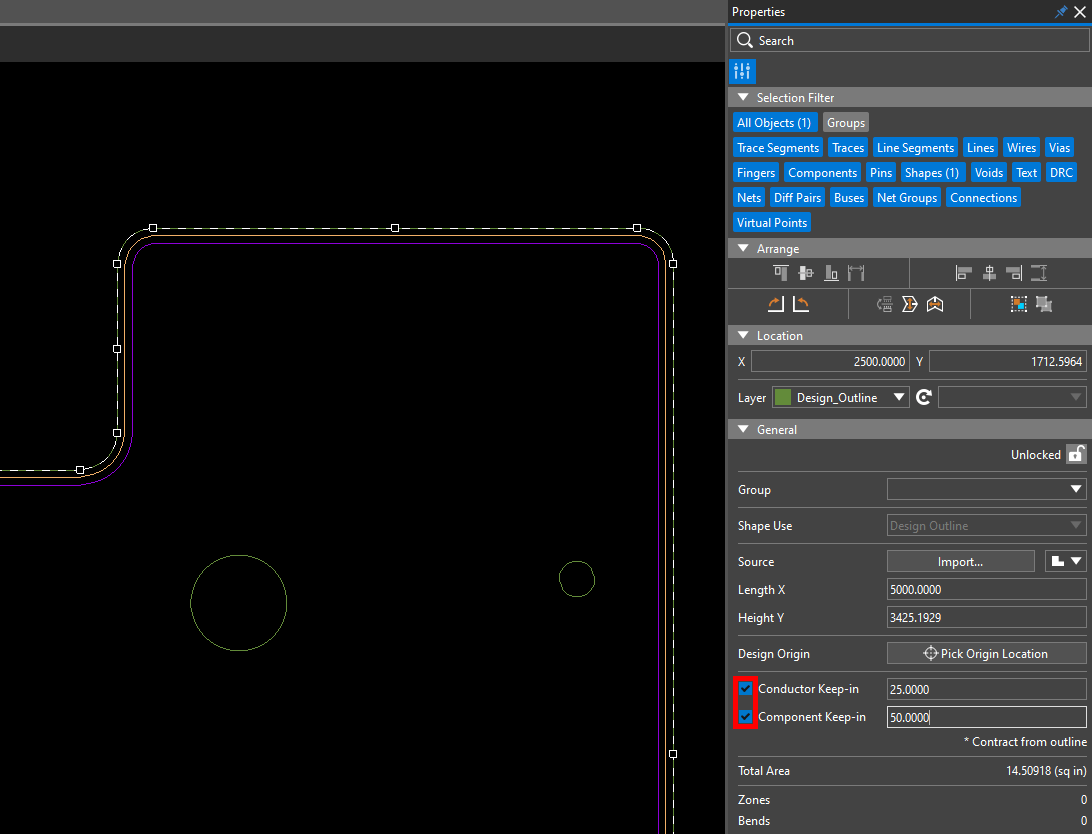
The route keepin is used in Allegro X AI to calculate the board area and density. This should be defined when creating the board outline for accuracy when computing the area and density of the design.
If not present, “design outline” is used for the computation of the board area and density.
Define Spacing Constraints
Location: PCB Canvas
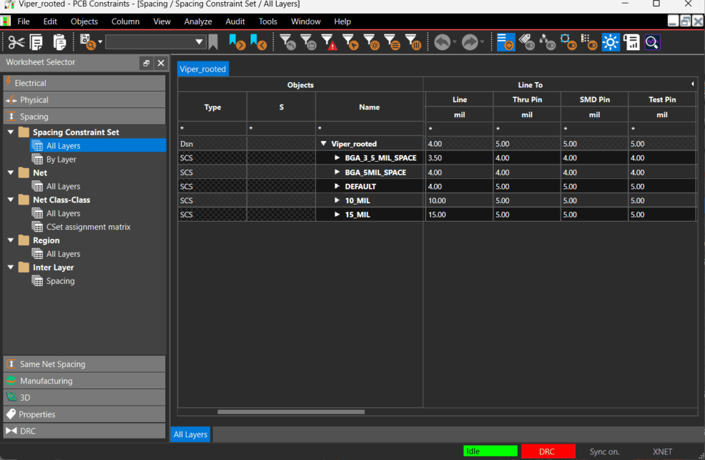
Define and assign important spacing constraints for the design in constraint manager. Allegro X AI will understand the constraints configured in constraint manager and take them into consideration when placing parts. For part placement, the following spacing and same net spacing constraints are supported by Allegro X AI:
- Line to
- Thru Pin to
- SMD Pin to
