
Adjust Grid Sizes for Component Placement: Non-Etch Grids
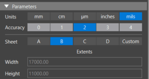
Step 1: Open the desired design or the provided design in OrCAD X Presto. Before settings grids, verify the units of your design in the Properties panel. The grid will be set based on these units.
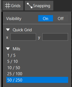
Step 2: Select Grids. Here you have the ability to turn visibility on and off, configure grids based on the preconfigured default values, or define custom grids.
Step 3: Set the Visibility to ON. This will enable us to see the differing grid spacing on the PCB canvas.
Step 4: Select the preconfigured value of 50/250 mils from the grid spacing list. The grid has been updated in the PCB canvas.
Configuring Snapping for Component Placement
The following steps show how to automatically snap to grids when placing components or other design elements.
Step 5: Select Snapping.
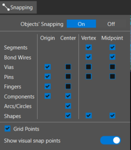
Step 6: Turn Object Snapping On.
Step 7: Ensure the proper snapping configuration for components and other design elements. For this example, select Origin and Center for component snapping.
Step 8: Select Grid Points.
Step 9: Select the Snapping tab again to close the panel.
Verifying Grids for Component Placement
Step 10: Right click on the move icon in the toolbar and select component placement.
Step 11: Select a component from the search panel. Move the cursor. The component snaps to each grid point. Click to place the component.
Creating Custom Grids in OrCAD X
Step 12: Click the Grids tab.
Step 13: In the Quick Grid section, enter 5 mils for the X Value and press TAB on the keyboard. The Y value is automatically populated with the same value. Press Enter.
Step 14: Select the Grids tab again to close the panel.
Step 15: Select another component from the search panel. The component now snaps to the smaller grids for greater accuracy and control during placement.
Adjust Grid Sizes for Component Placement: Non-Etch Grids
Step 1: Open the desired design or the provided design in OrCAD X PCB Editor.
Step 2: Select Setup > Design Parameters from the menu. Select the Design tab.
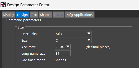
Step 3: View the units for the design. The grid settings will be configured based upon the design units. Click OK.
Step 4: Setup > Grids from the menu. Here you can turn grids on and configure the values for non-etch and etch grids.
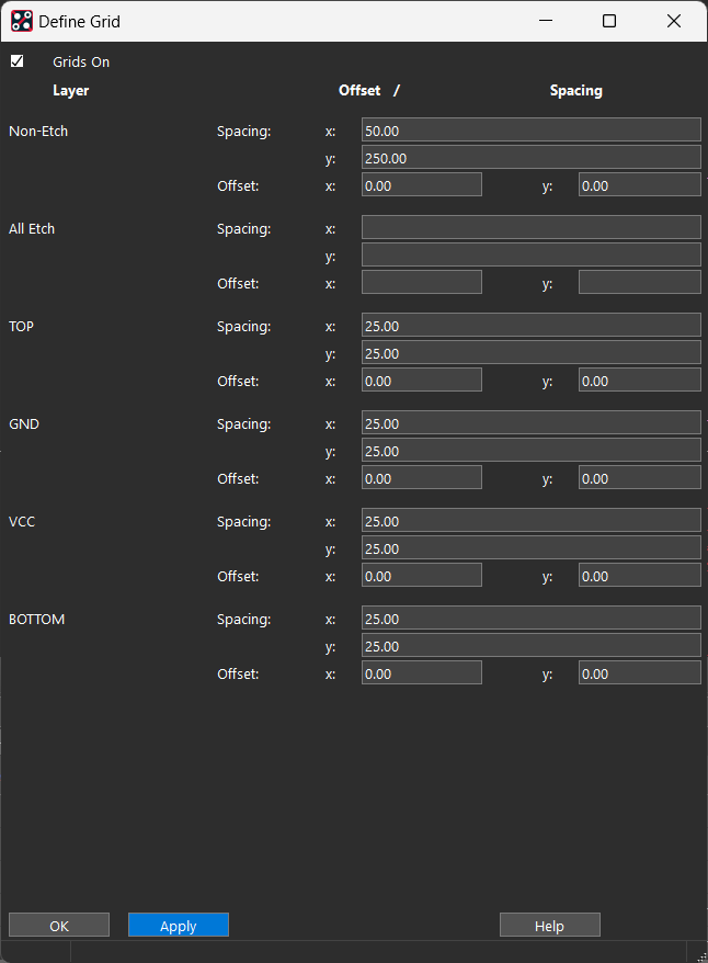
Step 5: Check the box to turn grids On.
Step 6: For the non-etch grid, set the X to 50 and the Y to 250. Select Apply and OK.
Verifying Grids for Component Placement
Step 7: Select the Move icon from the toolbar.
Step 8: Select a component. Move the cursor. The component snaps to each grid point. Click to place the component.

