

While PCB designers and fabricators can work to get as close to perfect values as possible, there will always be some deviation. With today’s high-speed and ever-more compact designs, the allowed tolerance for physical dimensions such as dielectric thickness must be specified explicitly. In Allegro X PCB Designer, quickly and easily define tolerances for hole sizes and dielectric thicknesses to ensure your design remains within the required specifications.
This quick how-to will provide step-by-step instructions on how to configure tolerances for holes and dielectric thickness in Allegro X.
To follow along, download the provided files above the table of contents.
How-To Video
 Open in New Window
Configure Tolerances in Allegro X: Hole Tolerance
Step 1: Open the provided design in Allegro X PCB Designer.
Step 2: Tolerance for drilled holes can be defined through the Padstack Editor. Select Tools > Padstack > Modify Design Padstack from the menu.
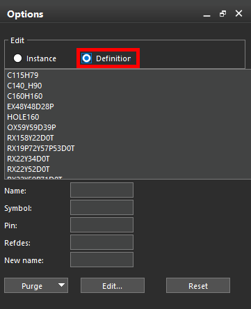
Step 3: The Options panel shows the list of padstacks in the design and fields for name, symbol, and pin. Select Definition under Edit to configure options for all instances of the selected padstack.
Step 4: Select one of the mounting holes on the board. The Name field is automatically populated with the padstack name: HOLE160.
Step 5: Select Edit to open the Padstack Editor.
Configuring the Drill Tolerance
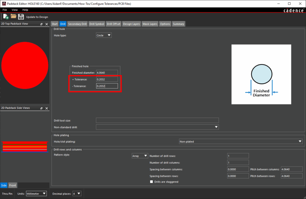
Step 6: The Padstack Editor opens to show settings for the HOLE160 padstack. To set the tolerance, select the Drill tab.
Step 7: The Finished Hole section under Drill Hole lists the finished diameter of the hole and its tolerance. Currently, both tolerance fields are set to 0. Enter 0.2032 for both fields for a 5% tolerance in both directions.
Step 8: Select Update to Design to push the change to the PCB canvas.
Step 9: A warning message appears saying that increasing the drill hole size may lead to pad breakout. Click Close to ignore this warning.
Step 10: When prompted to update, click Yes.
Step 11: Close the Padstack Editor.
Step 12: Right-click and select Done to commit the changes.
Configure Tolerances: Multiple Drill Tolerances
Step 13: Multiple hole tolerances can be configured simultaneously if desired. To do this, select Manufacture > NC > Drill Customization from the menu.
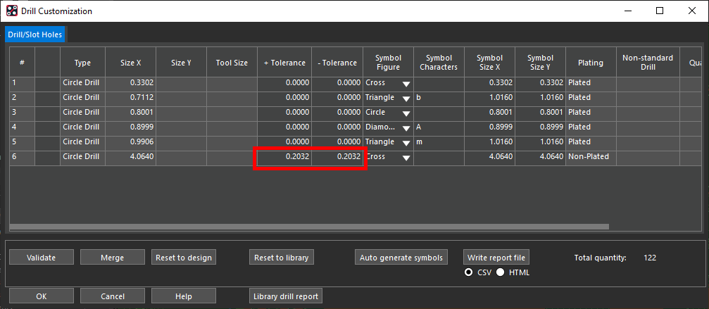
Step 14: The Drill Customization window opens. The screw holes edited earlier are the only non-plated components in the list. Confirm that the positive and negative tolerances are set correctly.
Step 15: Enter the following tolerances for each plated hole.
- Size 0.3302: 0.0165
- Size 0.7112: 0.0355
- Size 0.8001: 0.0400
- Size 0.8999: 0.0449
- Size 0.9906: 0.0495
Step 16: Select Validate to validate the drill sizes.
Step 17: Click OK to save the settings and close the window. Click Yes when prompted to update the padstacks.
Configure Tolerance: Dielectric Thickness
Step 18: To configure dielectric thickness tolerance, select Setup > Cross-section from the menu.
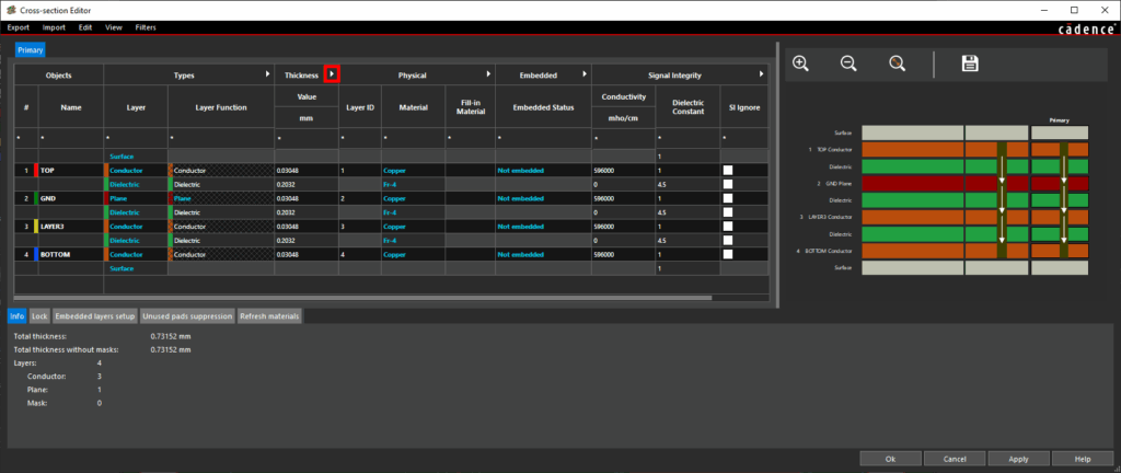
Step 19: The Cross-Section Editor window opens, displaying the board stackup. Double-click the arrow in the Thickness column header to expand it.
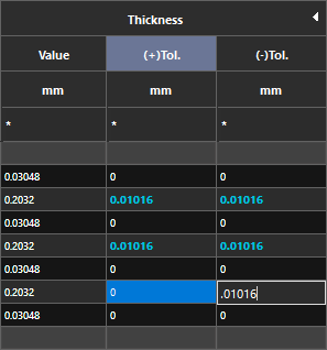
Step 20: The Thickness column expands to show new columns for positive and negative tolerance. Click and drag to select the tolerance cells for the dielectric between TOP and GND to edit them.
Step 21: Enter 0.01016 for the tolerance. Click outside the cells. The value is assigned to both.
Step 22: Click and drag to select the tolerance cells for the dielectric between GND and LAYER3. Enter 0.01016 and click outside the cells.
Step 23: Click and drag to select the tolerance cells for the dielectric between LAYER3 and BOTTOM. Enter 0.01016 and click outside the cells.
Step 24: A tolerance has been assigned to each dielectric. Click OK to save the stackup configuration and close the window.
Wrap Up & Next Steps
Quickly define and configure tolerances for drill holes and dielectric thickness to ensure correct functionality in your PCB designs with Allegro X. Get more how-tos for Allegro X at EMA Academy.

