
Fix Mounting Holes in OrCAD X
Mounting holes should be fixed within the PCB layout to prevent movement during the layout process and to ensure proper integration with the mechanical housing.
Step 1: Open the provided design in OrCAD X Presto.
Step 2: Click to select a mounting hole on the PCB. Hold down CTRL and select the remaining mounting holes.
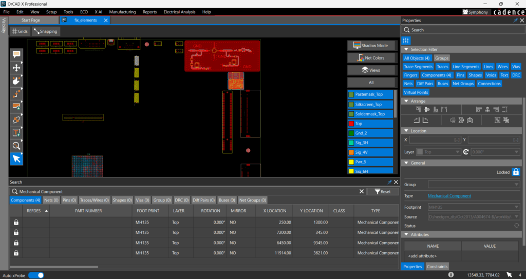
Step 3: In the Properties panel, select the Lock icon. The lock turns blue indicating these are now fixed elements on the PCB.
Step 4: To verify all mechanical components have been locked, select the hyperlink for Mechanical Components. The search panel opens, pre-filtered to only show the mechanical components. All elements are locked as indicated in the first column. Select Reset to reset the filters.
Fix Components in OrCAD X
Important components, such as main ICs, and components which will interfere with the mechanical housing such as connectors, switches, and LEDs should also be fixed in the PCB to prevent errors.
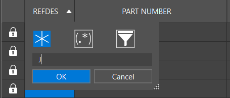
Step 5: In the Search Panel under REFDES, select the Filter icon. In the wildcard filter, enter J and click OK.
Step 6: View the Search panel. The design information has been filtered to only show components with reference designators containing J.
Step 7: Select the Lock icon in the first column of the search panel for each of the connectors listed.
Step 8: Select the Filter for the reference designator again. In the wildcard filter, select U and click OK.
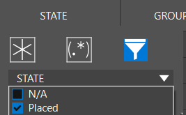
Step 9: Select the Filter for the State. Select the filter icon again. In the drop-down menu, select Placed and click OK.
Step 10: The Search panel displays the ICs with reference designator U that are placed on the PCB. Click the lock icon for each returned search result.
Step 11: Select XP1 at the bottom of the board. In the Properties panel, select the lock icon to fix the element on the PCB.
Fix RF Circuits in OrCAD X
Critical elements, such as RF circuitry and intricate layouts, must be locked to ensure proper operation.
Step 12: In the Search panel, select Reset to clear the configured filters.
Step 13: In the search bar, type RF and select Enter. The components in the RF circuitry have been returned. Some components have been locked and cannot be modified as indicated with the grayed-out lock in the search panel.
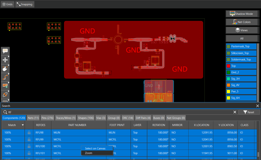
Step 14: Press CTRL + A to select the returned results then right-click and choose Select on Canvas. View the RF circuitry.
Step 15: Hold down CTRL and select the ground shape encompassing the RF circuitry.
Step 16: In the Properties panel, the Lock icon has an ellipsis next to it indicating some of the selected components are locked. Select the lock icon to fix the entire selection.
Fix Critical Routing and Fanouts in OrCAD X
Sensitive traces, fanouts for BGAS, and other traces that are critical to the functionality of the PCB can also be locked into place to prevent movement. This is especially important if using interactive and advanced routing features such as shove which may move traces to accommodate other routing.
Step 17: In the Selection filter, select All Objects to deselect all objects, then select Components, Traces and Vias. This will allow you to only select components, traces, and vias in the PCB canvas.
Step 18: Navigate to U37 using the arrow keys on the keyboard or wheel on the mouse. Highlight U37 as well as the vias in the fanout. In the properties panel, select the lock icon to lock the fanout in place.
Step 19: Navigate to the routed traces for U1.
Step 20: In the Selection filter, select off of components then select the traces by clicking and dragging in the PCB canvas. In the properties panel, select the lock icon to lock the traces in place and prevent modifications.

Fixing Mounting Holes in OrCAD X
Components and mounting holes can be fixed during placement using the following method.
Step 1: Open the provided design in OrCAD X PCB Editor.
Step 2: Select General Edit in the bottom toolbar and choose Placement Edit.
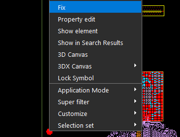
Step 3: Hover the mouse over a mounting hole on the PCB. Right-click and select Fix.
Step 4: Complete this process for the remaining three mounting holes.
Fixing Components in OrCAD X
To save time and reduce mouse clicks, all critical components can be fixed at once after placed in their required locations on the PCB.
Step 5: Select Placement Edit in the bottom toolbar and choose General Edit.
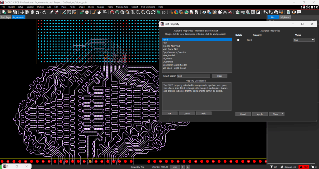
Step 6: Select Edit > Object Properties from the menu.
Step 7: The Find filter is automatically activated. Turn All Off then select Comps.
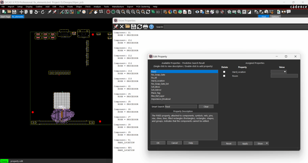
Step 8: Click and drag to highlight a section of the board, avoiding the RF circuitry at the top.
Step 9: The Show Properties window appears listing all the selected components as well as the Edit Properties window. In the Smart Search, type Fixed and press Enter.
Step 10: Double-click Fixed to associate the property, then select Apply and OK.
Step 11: Highlight another section of the PCB, avoiding the RF circuitry at the top.
Step 12: In the Smart Search box in the Edit Properties window, type Fixed and press Enter.
Step 13: Double click Fixed to associate the property, then select Apply and OK.
Fix Critical Routing and Fanouts in OrCAD X
Sensitive traces, fanouts for BGAS, and other traces that are critical to the functionality of the PCB can also be locked into place to prevent movement. This is especially important if using interactive and advanced routing features such as shove which may move traces to accommodate other routing.
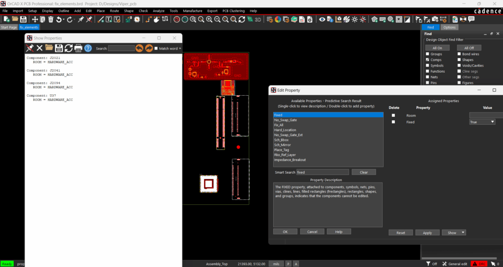
Step 14: In the Find panel, uncheck Comps and select Vias.
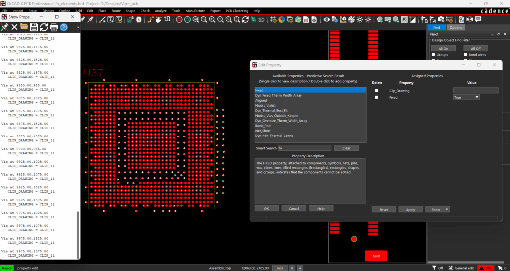
Step 15: Highlight the fanout around U37.
Step 16: In the Smart Search bar in the Edit Properties window, type Fixed and press Enter.
Step 17: Double-click Fixed to associate the property, then select Apply and OK.
Step 18: In the Find panel, uncheck Vias and select Clines.
Step 19: Highlight the traces around U1.
Step 20: In the Smart Search bar in the Edit Properties window, type Fixed and press Enter.
Step 21: Double-click Fixed to associate the property, then select Apply and OK.
Fix RF Circuits in OrCAD X
Critical elements, such as RF circuitry and intricate layouts, must be locked to ensure proper operation.
Step 22: In the Find panel, uncheck Clines and select Symbols.
Step 23: Highlight the RF circuitry at the top of the board. The Show Property panel opens. The RF components and symbols are shown as locked. It is recommended to use the Locked property for a group of objects. Click OK in the Edit Properties window.
Step 24: The components and via shielding in this RF circuitry are not fixed or locked yet. To complete this, uncheck symbols and select Comps and Vias in the Find panel.
Step 25: In the Smart Search bar in the Edit Properties window, type Fixed and press Enter.
Step 26: Double-click Fixed to associate the property, then select Apply and OK.
Step 27: Right-click and select Done (F6).
Step 28: The shape around the RF circuitry can also be fixed or frozen to prevent modification. Select Shape > Freeze Shape(s) from the menu.
Step 29: Select the ground shape, then right-click and select Done.
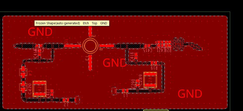
Step 30: In the Find filter, select All On. Hover the cursor over the shape to verify the dynamic shape is now frozen.

