As Qualcomm expands into new products and industries, the number of PCB projects is rising rapidly. To stay ahead in a fast-moving technology market, the development team must deliver a high volume of high-quality designs in less time. Nearly half of these projects are classified as low to medium complexity—boards with fewer than 5,100 components and a pin density below 100 pins/cm².
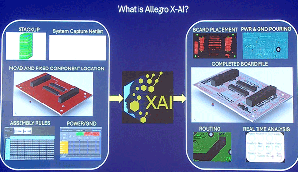
To meet tight schedules for these designs, Qualcomm turned to X AI. The approach centers on providing the AI engine with critical, intelligently defined inputs so it can automate much of the layout work while maintaining design integrity. Designers supply:
- Electrical Data: stack-up details, netlist, and power/ground requirements
- Mechanical Data: fixed component locations, MCAD constraints such as height limits and mounting holes
- Assembly Data: fabrication and assembly rules
Armed with this information, X AI generates a complete board file—including component placement, copper pours for power and ground, routing, and real-time layout analysis—dramatically accelerating the path from concept to manufacturable PCB.
Challenges
Before adding X AI to your PCB design process, it’s essential to lay the right groundwork. AI can dramatically accelerate layout and optimization, but its benefits only reach their full potential when key concerns are addressed up front. For Qualcomm, implementing an AI tool for PCB design required protecting intellectual property, securing sensitive data, and ensuring every layout met strict electrical, mechanical, and manufacturing standards.
The following considerations outline the primary challenges—and the built-in safeguards—that ensure X AI enhances productivity without compromising confidentiality, compliance, or design quality.
1. Protecting Intellectual Property
Challenge: Intellectual Property (IP) is of the utmost importance in the technological industry, especially with AI involvement. Companies must ensure their IP is protected and not used to train AI engines, providing insights to other companies.
Solution: With X AI, customer designs and IP are NOT sent back to Cadence. Additionally, customer data is not used to train or improve the AI engine.
2. Data Security
Challenge: Industries like defense, medical, and automotive must meet strict cybersecurity and export-control standards, complicating AI adoption.
Solution: ISO 27001 certificate confirms commitment to information security and ensures data is safe and secure. Additionally, X AI offers on-premises and/or cloud solutions to adhere to company’s requirements.
3. Design Accuracy
Challenge: AI is often trained on incomplete or unrepresentative PCB datasets can generate layouts that miss critical manufacturing or signal-integrity constraints. Designers must still perform extensive simulation and design-rule checking to ensure AI outputs meet performance, safety, and regulatory standards.
Solution: Allegro X AI consists of traditional hardware algorithms as well as an AI engine and is pre-trained using open-source designs. Constraints that are supplied to Allegro X AI ensure that the design meets the mechanical, electrical, and manufacturing requirements. With embedded constraints and real-time analysis, design verification is accelerated.
4. Managing Design Requirements
Challenge: AI results are heavily dependent upon the requirements and constraints provided. It is essential that critical design information is communicated effectively and defined clearly for AI tools to use to generate an accurate PCB layout.
Solution: X AI integration within Cadence Design Solutions enables designers to leverage the capabilities of System Capture to clearly define and manage the design intent. System Capture is a modern schematic entry tool which allows for hierarchical design and helps nets to be logically grouped based on function, voltage level, or power domain. The additional integration enables:
-
-
- A netlist consisting of enhanced data that supports Allegro X AI advanced placement algorithms, such as associating decoupling capacitors with the corresponding IC and intelligently placing these components near the appropriate pins.
- Room property definition that will automatically update to the layout once the netlist is imported.
- Minimal migration and translation efforts as no library changes are required.
-
By addressing these challenges head-on, Qualcomm created a solid foundation for AI integration and with these safeguards in place, the focus could shift from potential risks to measurable results. These results revealed how X AI translated careful preparation into faster layouts, higher efficiency, and consistently reliable designs.
Results
Qualcomm had great success implementing X AI for their low to medium complexity designs. X AI was able to run in the background while designers were completing other work or more important jobs. X AI produced results quickly including board placement, power and ground pouring, and routing.
Board Layout
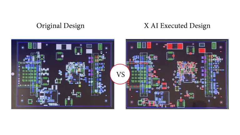
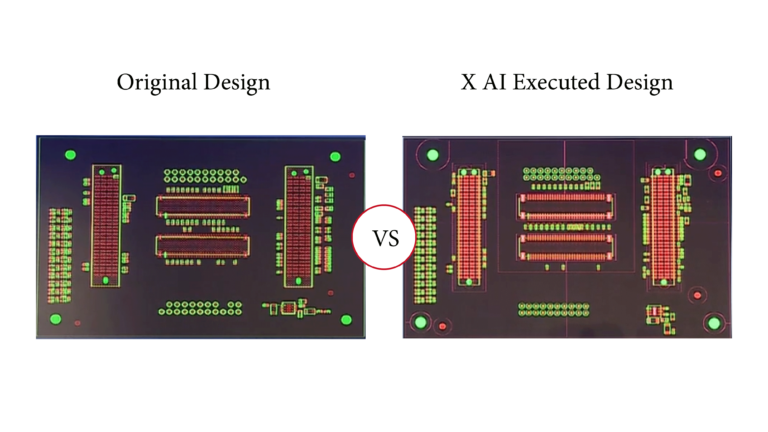
X AI was tested on original Qualcomm designs to test the time saving opportunity as well as the functionality and accuracy of the generated layouts. X AI was able to generate similar layouts to the originals, adhering to the functional and manufacturing requirements set forth by the designers. The following stats were obtained from the board layout testing:
| Completion | AI Run Time | Additional Design Time |
|
| Design 1 | ~97% | 4 Minutes | 1 - 1.5 Hours |
| Design 2 | 100% | 6 Minutes | 2 - 3 Hours |
Copper Pours

For copper pour generation with X AI, providing accurate current and voltage ratings for each power net is a critical first step. These electrical parameters enable the AI engine to calculate the optimal copper width and determine the most appropriate layer allocation for each net, ensuring that both electrical performance and thermal dissipation requirements are met.
X AI’s approach to power plane generation goes beyond simple layout automation. The tool performs early-stage analysis of voltage drop and current density to identify potential hotspots and ensure uniform power delivery across the board. This preemptive evaluation allows the AI to make informed decisions about layer assignments and copper distribution, maintaining power integrity throughout the design.
Routing
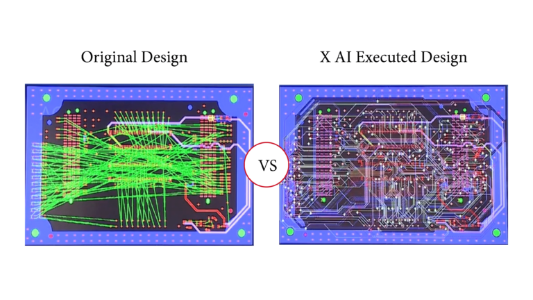
X AI contains a powerful routing engine allowing engineers to define the routing requirements including, routing layers, delay and phase tuning, bump length, differential pair and matched group rules, and advanced routing options. Designers can then define what type of routing should be completed, selecting from:
- 100% Connection: X AI will achieve complete routing and ignore any design rule errors
- ECO routing: X AI will route a portion of the board that needs to be modified
- Routability Estimation: X AI will estimate how much of the board can be routed with current component placement
- Maximize for Completion: X AI will complete as much routing as possible without creating design rule violations
With X AI, Qualcomm was able to complete the majority of their PCB routing quickly and then focus resources on the manual completion of critical traces and cleanup.
| AI Run Time | Additional Design Time |
|
| Design 1 | 6 Minutes | 2 - 3 Hours |
By implementing X AI into their PCB design flow, Qualcomm was not only able to free up engineering resources but was able to accelerate their PCB design process- saving up to 60-70% of vital design time.
Advantages of Allegro X AI
Integrating Allegro X AI into the PCB design workflow offers a range of benefits that go far beyond simple automation. By leveraging AI-driven capabilities, designers can explore multiple layout strategies, evaluate options quickly, and make more informed decisions—all while maintaining high standards for performance, manufacturability, and reliability.
The following advantages highlight how X AI transforms the design process, enabling faster iteration, optimized layouts, and greater overall productivity for engineering teams.
- Parallel Iterations: Allegro X AI enables designers to run multiple design iterations and layout strategies simultaneously, significantly improving workflow efficiency
- Placement & Routing Strategies: The Allegro AI-drive tool generates various component placement, routing, and plane methodologies, allowing engineers to explore multiple approaches effortlessly.
- Quick Turnaround Time: By automating the design process, Allegro X AI ensure a rapid evaluation of different placement strategies, reducing manual effort.
- Optimized Design Selection: Engineers can analyze and compare different placement, routing, and copper pour methodologies to select the most effective one based on performance, manufacturability, and reliability.
- Enhanced Productivity: With Allegro AI-driven automation, designers can focus on innovation rather than manual layout adjustments, accelerating PCB development cycles.
“Tasks that previously took designers around 20 days can now be completed in just 2 days.”
Dhivagar M., Developer, Qualcomm
Accelerating PCB Development Through AI-Driven Automation
By integrating Allegro X AI into its PCB design workflow, Qualcomm successfully addressed key challenges—protecting intellectual property, securing sensitive data, and ensuring design accuracy—while significantly accelerating design cycles. For low to medium complexity boards, X AI automated component placement, copper pours, and routing, enabling engineers to focus on high-value tasks and critical design decisions.
The results speak for themselves: X AI delivered accurate layouts that adhered to functional and manufacturing requirements, reduced manual effort, and cut design time by up to 60–70%. Its capabilities—parallel iterations, multiple placement and routing strategies, and rapid evaluation of design options—empowered Qualcomm to explore optimized solutions efficiently.
Ultimately, Allegro X AI demonstrates how AI-driven automation can transform PCB design, providing faster turnaround, enhanced productivity, and consistent quality while maintaining strict compliance with electrical, mechanical, and manufacturing standards. As Qualcomm continues to expand into new products and industries, X AI provides a scalable, secure, and intelligent foundation for meeting the growing demands of modern PCB development.
This customer success story was presented as part of CadenceLive India 2025. Get a recap of this inspirational day where over 2,500 visionaries from electronics and AI gathered to learn about the advancements in the industry here.
