Modern electronics could not exist without semiconductors and digital electronics but as electronics become faster and more complex, it’s essential to model realistic behavior to ensure design accuracy. At high speeds, digital electronics are susceptible to issues with propagation delay, and any stray capacitance present on the board could lead to attenuation, which could prevent a high input from ever reaching the device’s threshold voltage. PSpice allows you to quickly create a custom SR flip-flop SPICE models for accurate simulation of digital designs with a wizard-based approach.
This quick how-to will provide step-by-step instructions on how to create a clocked SR flip-flop SPICE model in OrCAD PSpice.
To follow along, download the materials provided above the table of contents.
How-To Video
 Open in New Window
Creating an SR Flip-Flop SPICE Model
Step 1: Open the provided design in OrCAD PSpice 23.1.
Note: A wizard-based approach to digital models is new in version 23.1. See other new features here.
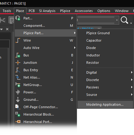
Step 2: Select Place > PSpice Part > Modeling Application from the menu.
Step 3: In the Modeling Application, expand Digital > Flip Flops.
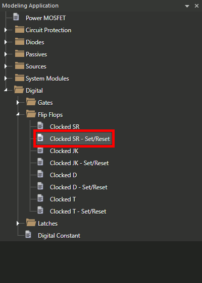
Step 4: Select Clocked SR – Set/Reset.
Note: This model contains PRESET and CLEAR pins, which can be used to set the output of the flip-flop without the clock.
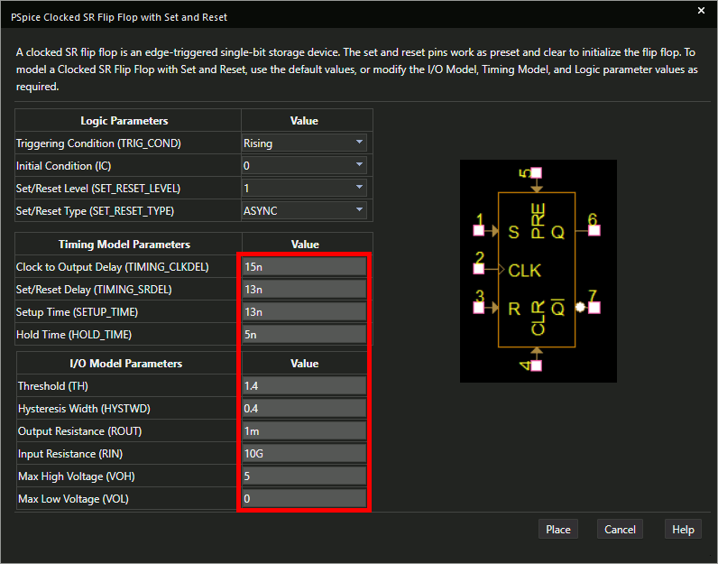
Step 5: The Clocked SR Flip-Flop options window opens. Enter the following model parameters:
- Clock to Output Delay: 15n
- Set/Reset Delay: 13n
- Setup Time: 13n
- Hold Time: 5n
- Threshold: 1.4
- Hysteresis Width: 0.4
- Output Resistance: 1m
- Input Resistance: 10G
Note: The logic device being modeled has negligible output resistance and requires negligible input current.
Step 6: Click Place.
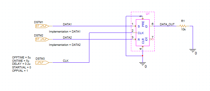
Step 7: Click to place the flip-flop in the schematic.
Step 8: Select the Voltage/Level Marker button from the toolbar.
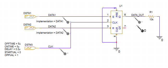
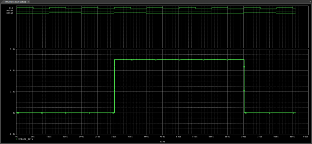
Step 9: Click to place probes on the CLK, DATA1, DATA2, and DATA_OUT nets. Right-click and select End Mode when finished.
Running the Simulation
Step 10: Select PSpice > Run from the menu.
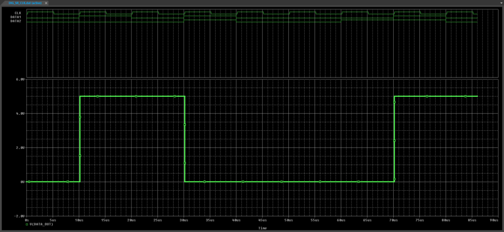
Step 11: View the simulation results.
Modifying the Design
Step 12: Back in the schematic, select the DSTM1 stimulus.
Step 13: Hold Alt on the keyboard and click and drag to disconnect the stimulus from the net.
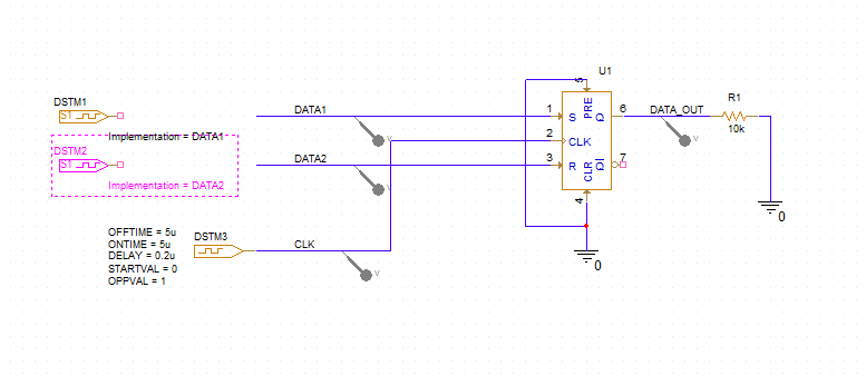
Step 14: Select the DSTM2 stimulus. Hold Alt and click and drag to disconnect the stimulus from the net.
Step 15: Click and drag DSTM1 to connect it to the DATA2 net.
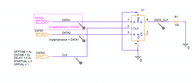
Step 16: Click and drag DSTM2 to connect it to the DATA1 net.
Step 17: Select PSpice > Run from the menu.
Step 18: View the simulation results.
Wrap Up & Next Steps
Quickly create the required SR Flip-Flop SPICE models and simulate accurate digital circuit behavior with the PSpice Modeling Application in OrCAD PSpice. Upgrade to the latest 23.1 release or test out this feature and more with a free trial of OrCAD.
