After completing the PCB Layout, the design cycle continues with fabrication, assembly, verification, and testing. It is essential to update reference designators for components according to the PCB Layout for peak efficiency in the manufacturing and testing process. Component reference designators should read from left-to-right and top-to-bottom, for improved readability and quick component identification. However, some components (such as connectors and test points) will need to remain the same for documentation purposes.
This how-to provides step-by-step instructions to quickly update reference designators on the PCB while preserving critical component silkscreen using OrCAD PCB Designer.
How-To Video
Improve Visibility
Step 1: Open the Color Dialog Window, either by clicking the Color button on the toolbar or Setup > Colors from the menu.
Note: If desired, select Zoom Fit on the toolbar to center the PCB within the canvas.
Step 2: Turn Global Visibility off.
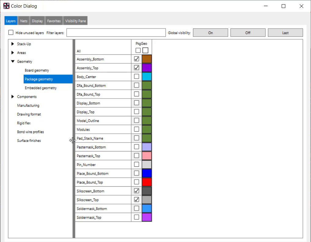
Step 3: In the Layers tab, under Geometry > Package Geometry, turn visibility on for Assembly_Bottom, Assembly_Top, Silkscreen_Bottom, and Silkscreen_Top.
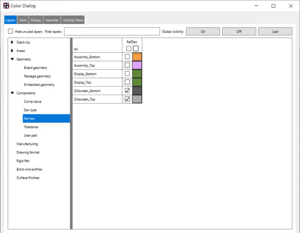
Step 4: Under Components > Ref des, turn visibility on for Silkscreen_Bottom and Silkscreen_Top.
Step 5: Click Apply and OK to close the window.
Note: This will improve visibility to only see the reference designators and component outlines.
Define Grids
Step 6: Select Setup > Grids from the menu. Check Grids On if it is not checked already.
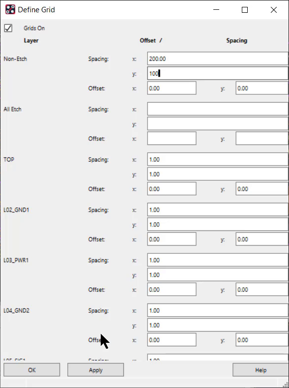
Step 7: Set the Non-Etch grid spacing to 200 in x, and 100 in y. Click Apply and OK.
Note: OrCAD uses the grid to determine the position of each part, which in turn determines the proper order for the new reference designators.
Renaming Reference Designators
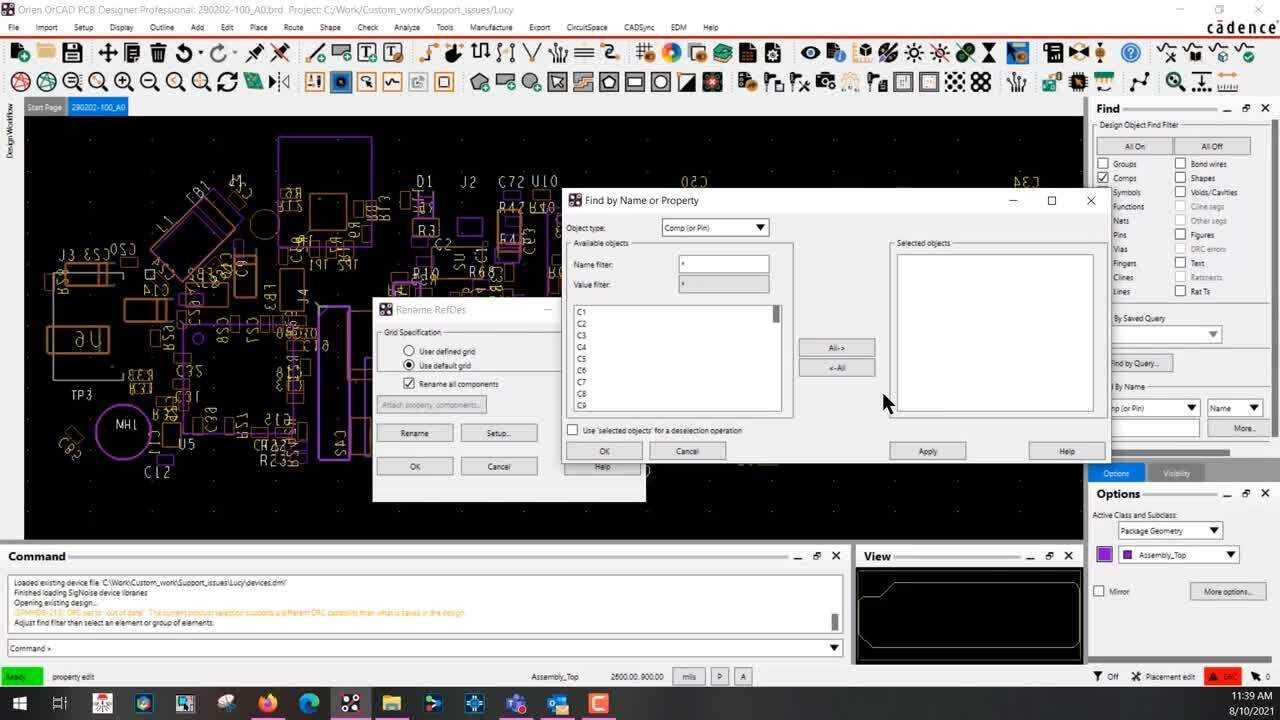
Step 8: Select Manufacture > Auto Rename Refdes > Rename. The Rename Refdes window will open.
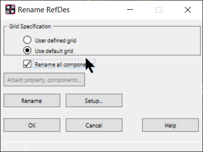
Step 9: Select Use default grid and check Rename all components.
Step 10: Without closing the Rename Refdes window, select Edit > Object Properties from the menu.
Selecting RefDes to Rename
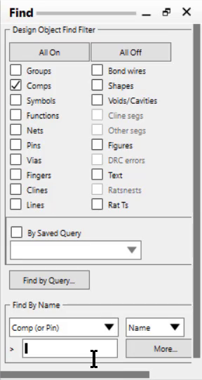
Step 11: In the Find window, under Find By Name, select Comp (or Pin).
Step 12: In the Find window, select More.
Step 13: Select All→ to move all objects to the Selected Objects list.
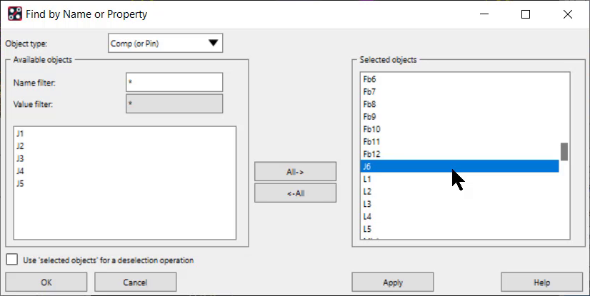
Step 14: Scroll down to find the components that you do not want updated. Click them to move them back to the Available Objects list.
Note: If you accidentally click a component that you want updated, simply click it again in the Available Objects list to move it back.
Step 15: Click Apply. This will open the Edit Property window.
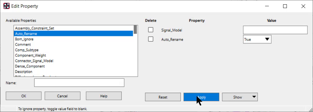
Step 16: Select Auto_Rename from the list of available properties. Make sure the value is set to True.
Step 17: Click Apply and OK.
Step 18: Back in the Find by Name or Property window, click the ←All button to move all of the components back to the Available Objects list.
Excluding Components
Step 19: Click the components that you do not want updated to move them to the Selected Objects list. Click Apply.
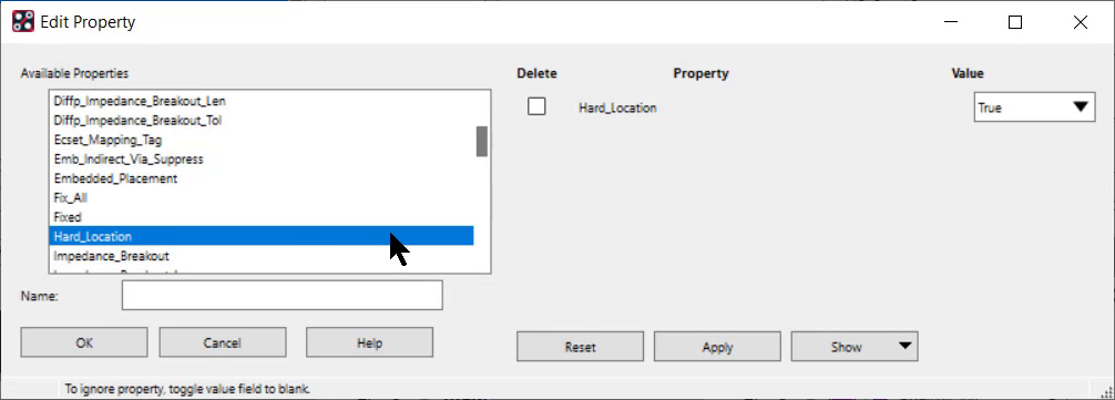
Step 20: Scroll down in the list of available properties and select Hard_Location. Make sure the value is set to True.
Step 21: Click Apply and OK.
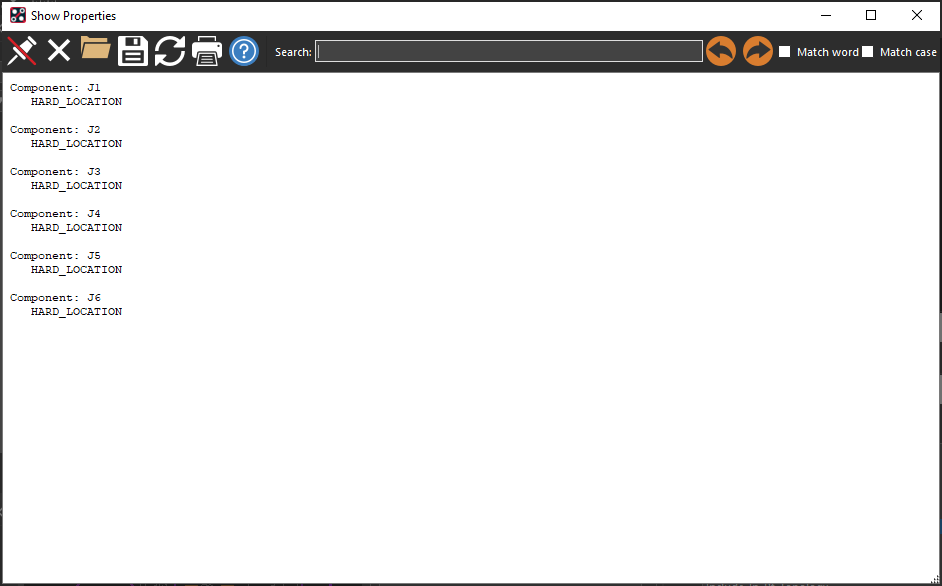
Note: The Show Properties window will open when you click Apply. Use this to confirm the desired properties have been set.
Step 22: Click OK to close the Find by Name or Property window.
Renaming Reference Designators
Step 23: In the Rename RefDes window, click Setup.
Step 24: Under Reference Designator Format, change the RefDes Prefix to an asterisk.
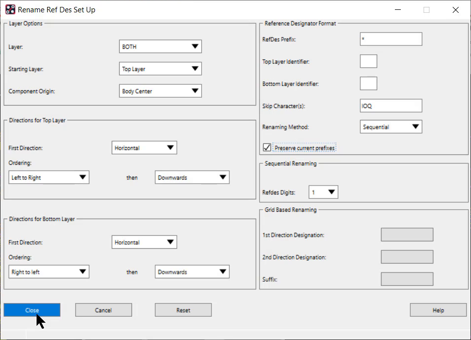
Step 25: Select Preserve current prefixes.
Note: Directions for the Top and Bottom layers are automatically set to reflect industry standards of left to right and top to bottom.
Step 26: Select Close.
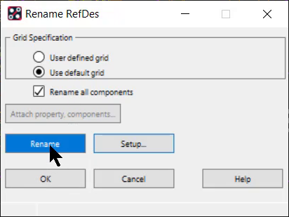
Step 27: Select Rename in the Rename RefDes window. Click OK to close.
Note: Now that the board has been re-sequenced, the changes must be pushed to the associated schematic. In OrCAD Capture, select PCB > Update Schematic. Verify the layout path and select Sync.
Wrap Up & Next Steps
Improve the readability of the PCB layout with easy reference designator updates in OrCAD PCB Designer and streamline component identification during assembly, inspection, and testing. For even more efficiency, utilize augmented reality with InspectAR to overlay crucial information including components and nets onto the PCB.
