Define Cross Section
Location: PCB Canvas
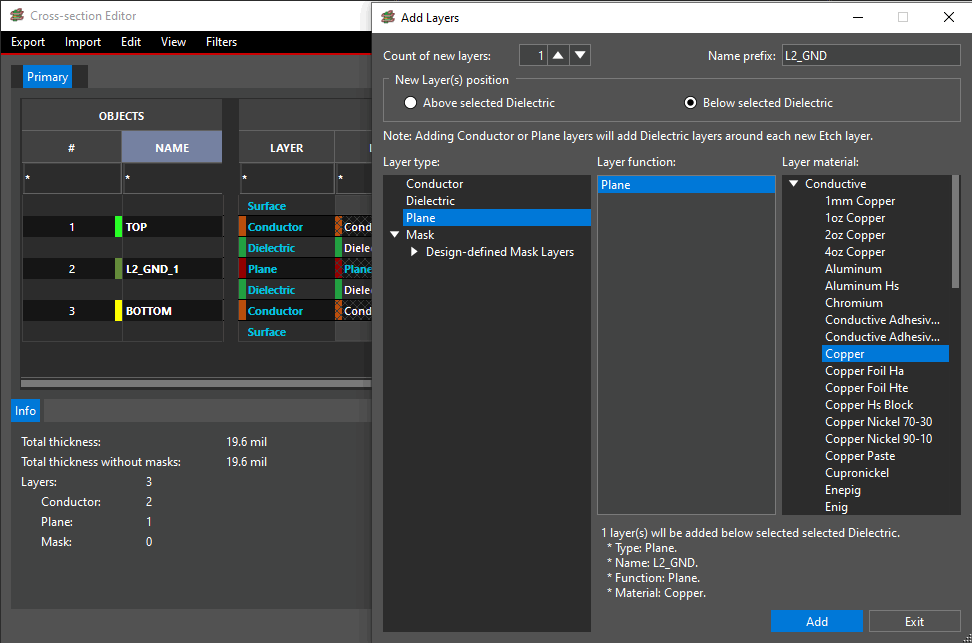
The cross-section should be created in OrCAD X or Allegro X by defining the conductor and plane layers in the PCB stackup. Additionally, all layers must have a thickness assigned.
Routing layers must be identified as conductor in the cross-section editor. The router will not route on layers defined as planes.
Need Help? Get step-by-step instructions for defining the cross-section here.
Define Route Keepins and Keepouts
Location: PCB Canvas
Define where routing is allowed on the PCB and certain areas where it is not with keepins and keepouts. Additionally, X AI uses the route keepin to determine the board area and density.
Define DC Nets
Location: PCB Canvas
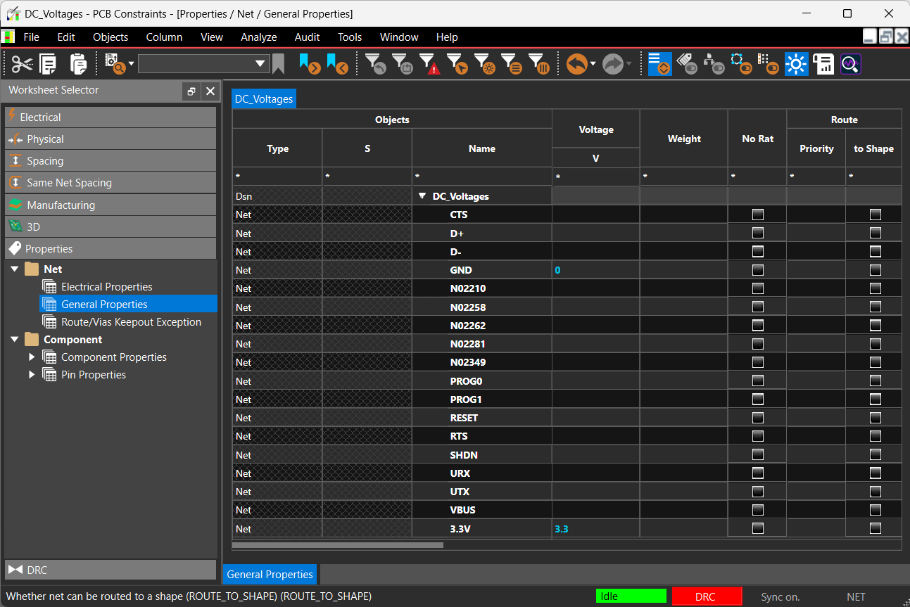
DC nets are defined by the DC voltage property and the Pin property (power defined on any pin of the net) in the constraint manager. These values will provide insight into connections to copper planes/pours and help to optimize the routing strategy.
Note: The router does not support routing/pin escapes of DC nets at this time.
Need Help? Get step-by-step instructions for defining DC voltage values here.
Completed Component Placement
Location: PCB Canvas
To properly route the connections between parts, all components must be placed inside the design outline.
Need Help? Get the step-by-step instructions for placing components here.
Define Differential Pairs
Location: Schematic or PCB Canvas
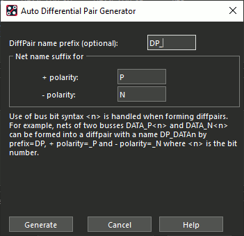
Define differential pairs in the PCB design. This includes defining the nets in the differential pair and groups them together. By defining the differential pairs, these traces will be routed together by X AI and additional rules can be configured to ensure proper functionality.
Need Help? Use these step-by-step instructions to learn how to define differential pairs in the schematic or PCB.
Define Physical Constraints
Location: PCB Canvas
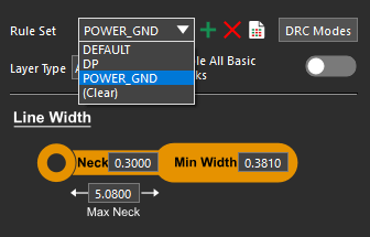
Physical constraints can be used to improve the results of routing with X AI. The following constraints are required:
- Minimum Line Width: The minimum line width constraint should not be too large for the pin escapes. Width values too large may cause DRCs at pin locations.
- Via List: Via lists can contain several candidates that would be leveraged during interactive routing.
