Sync the Board and the Schematic
Location: PCB Canvas or Schematic
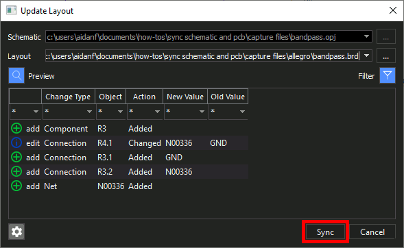
If information from the schematic has not been pushed to the PCB recently, users should sync the schematic and board files to ensure the correct information is communicated. Allegro X AI leverages this information to generate an optimized component placement. The critical information required from the schematic includes:
- The coordinates on the schematic
- Bounding box
- Mirror
- Component orientation
- Pin coordinates
Need Help? Get step-by-step instructions for synchronizing the PCB and schematic here.
Define Cross Section
Location: PCB Canvas
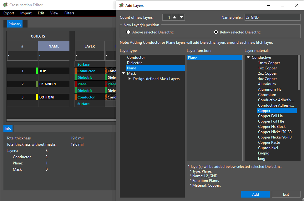
The cross-section should be created in OrCAD X or Allegro X by defining the conductor and plane layers in the PCB stackup. Additionally, all layers must have a thickness assigned.
Need Help? Get step-by-step instructions for defining the board stackup here.
Define Board Outline
Location: PCB Canvas
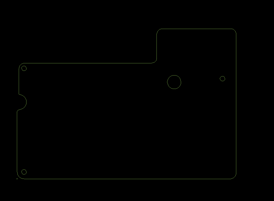
The shape and size of the PCB must be provided to Allegro X AI as this determines the area in which components can be placed. The board outline as well as any cutouts and holes should be defined to provide Allegro X AI with an accurate area for component placement.
Recommendations:
The recommended board size is less than 19″ x 32″.
Need Help? There are multiple ways to define the board outline in OrCAD X & Allegro X:
Import a DXF in OrCAD X PCB Editor
Import a DXF in OrCAD X Presto
Import an IDX in OrCAD X Presto
Draw a Board Outline in OrCAD X Presto
Define Package Keepins and Keepouts
Location: PCB Canvas
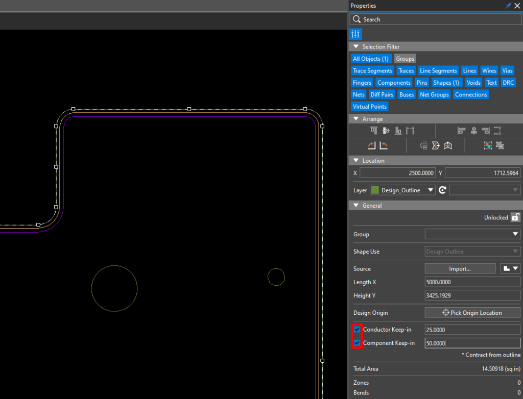
Define the areas on the board where components should and should not be placed with Package Keepins and Keepouts. Include height restrictions where required to properly interact with the mechanical housing.
Recommendations:
Include package keepouts on the top and bottom of the board around BGAs and other complex components to account for pin escapes.
Quick Place Components
Location: PCB Canvas
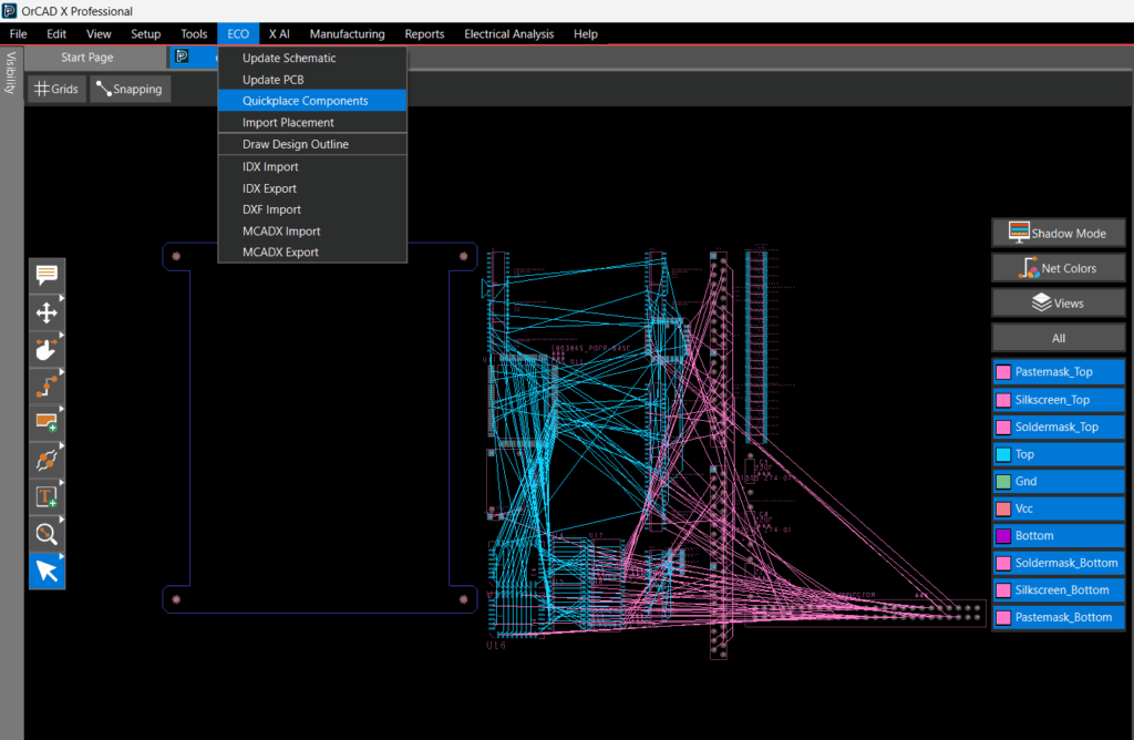
Allegro X AI does not read the Allegro symbol or pad library; therefore, components must be placed around the board outline.
Need Help? Get step-by-step instructions on how to quickly place components around the board outline here.
Grids
Location: PCB Canvas
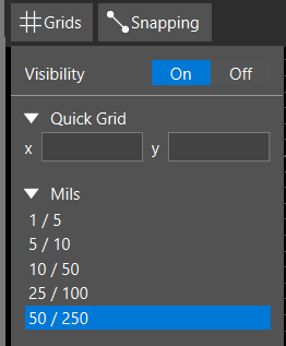
Check the Allegro Non-Etch Grid Setting as this applies to all components that will be automatically placed. Non-etch refers to the placement guides for all design elements except routing. If the grid is too small, component pins may overlap. If the grid is too large, there may not be enough space on the PCB to place all the components.
Recommendations:
Often designers will have standard grids for placing ICs and discretes. It is recommended to use the smaller grid, typically used for discrete component placement.
If no specific grid is necessary for your design, 5 mils or 0.127mm is recommended as a starting point.
Need Help? Get step-by-step instructions for configuring grids here.
Fix Mechanical / Key Components
Location: PCB Canvas
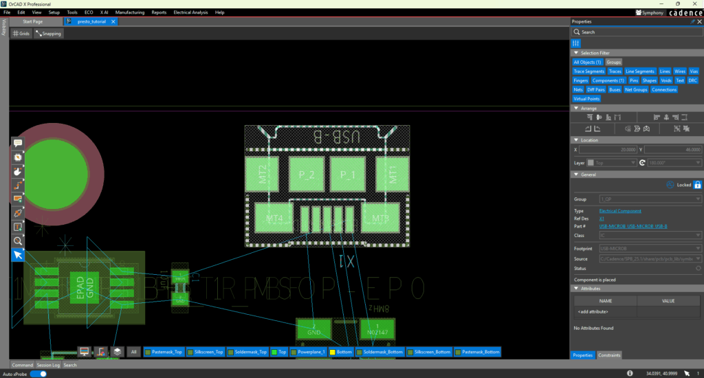
Critical components in the design that typically interact with the mechanical housing must be fixed as Allegro X AI does not have visibility into the full system design specifications and intent fixing, this includes:
- LEDs
- Connectors
- Switches
- Mounting Holes
Additionally, fixed IC placement is critical for improved quality, performance, and results. Aim to fix 1 to 2 large ICs such as BGAs, FPGAs, or other main components such as:
- Processor/Memory
- ASICs
- Transformers
Note: Allegro X AI will not automatically place mechanical components such as fiducials, labels, etc.
Recommendations:
Fix all connectors.
Fix all components that interact with mechanical housing.
Fix the important ICs in the design (1-2 ICs).
Assign DC Voltage Nets
Location: Schematic or PCB Canvas
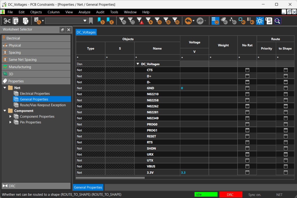
To assign DC Voltage Nets, define the voltage values for power and ground nets in the design. DC voltages should be assigned as properties in the constraint manager in OrCAD X or Allegro X or during schematic creation. This will automatically populate the values in the “Power and Ground” settings in Allego X AI. DC voltage nets are required for decoupling capacitor placement to identify which pin of the IC the capacitor needs to be placed close to.
Need Help? Get step-by-step instructions on how to assign DC Voltage nets here.
