Slots are often added to PCB footprints to adhere to mechanical and functional requirements including:
- Providing additional mechanical support
- Preventing damage to solder joints
- Ensure proper alignment of components during placement
- Incorporating heat sinking for high-power components
OrCAD X Presto makes it easy to add slots to a PCB footprint directly in the PCB canvas to quickly modify parts to meet your design requirements.
This quick how-to will provide step-by-step instructions on how to add slots to a PCB footprint with the Footprint Editor in OrCAD X Presto Professional.
To follow along, download the provided files above the table of contents.
How-To Video
 Open in New Window
Defining the Slot
Step 1: Open the provided drawing in OrCAD X Presto Professional.
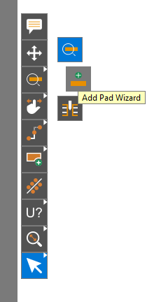
Step 2: Right-click Add Pin using Search in the toolbar and select Add Pad Wizard.
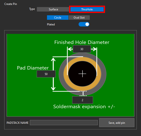
Step 3: The Create Pin widget opens. This widget allows you to create custom surface or through-hole padstacks. Select ThruHole for the Type to create a through-hole padstack.
Step 4: Select Oval Slot for the shape.
Step 5: Disable the Plated option to create a non-plated hole.
Note: Leave the option enabled to create a plated hole or pin.
Step 6: Enter 65 for the Slot Width X and 125 for the Slot Height Y.
Note: Normally, according to the provided datasheet, this footprint has round mounting holes with a diameter of 125mils. Since the mechanical mounts on the part are slightly flattened, this example will create slots of the same height but approximately half the width.
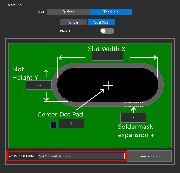
Step 7: Enter SS-7188V-A-NF_Slot for the Padstack Name.
Add Slots to a PCB Footprint in OrCAD X
Step 8: Click Save, Add Pin to add the pin to the footprint.
Step 9: The Pin Placement widget opens, showing the padstack name and options for the type of pin. Select Mechanical to place a mechanical pin with no number or electrical connection.
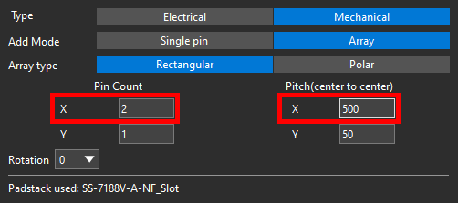
Step 10: Enter 2 for the X pin count and 500 for the center-to-center pitch.
Note: Since this example uses half-size slots instead of round holes, the centers are in different positions and must be adjusted accordingly.

Step 11: Click to place the pins at the bottom of the footprint to create the holes. Choose the Select mode from the toolbar to clear the cursor.
Adjusting the Slots
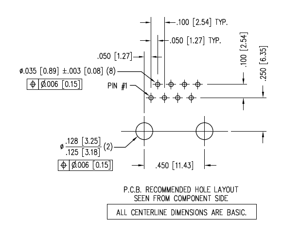
Step 12: According to the footprint diagram, the circular hole must be 50mil to the left and 250mil below the leftmost electrical pin.
Select the pin. The Properties panel shows it to be placed at (150,400).
Step 13: Select the non-plated slot on the left.
Since the circular hole must be 50mil to the left of the pin, the flattened slot must be 50mil plus half its width, or 80 mils to the left of the pin.
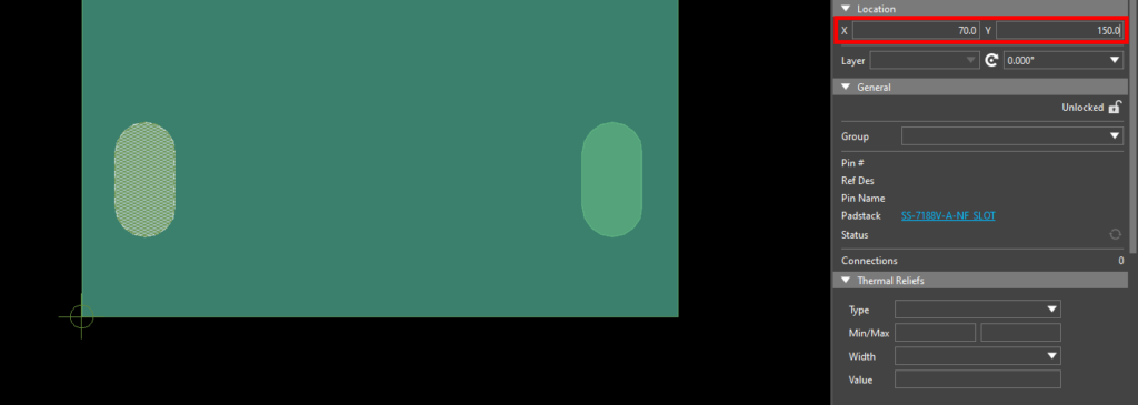
Step 14: In the Properties panel, under Location, enter 70 for the X location and 150 for the Y location. The slot is adjusted.
Step 15: Select the slot on the right. In the Properties panel, under Location, enter 580 for the X location and 150 for the Y location.
Checking the Footprint
Step 16: The footprint can be checked in 3D to verify the slot locations. Select Visibility to open the Visibility panel on the left side of the window.
Note: If the Visibility button is not present, select View > Panels > Visibility from the menu.
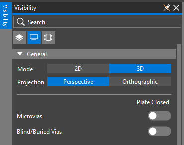
Step 17: Select the Display mode. Under General, select 3D for the Mode to enter the 3D view.
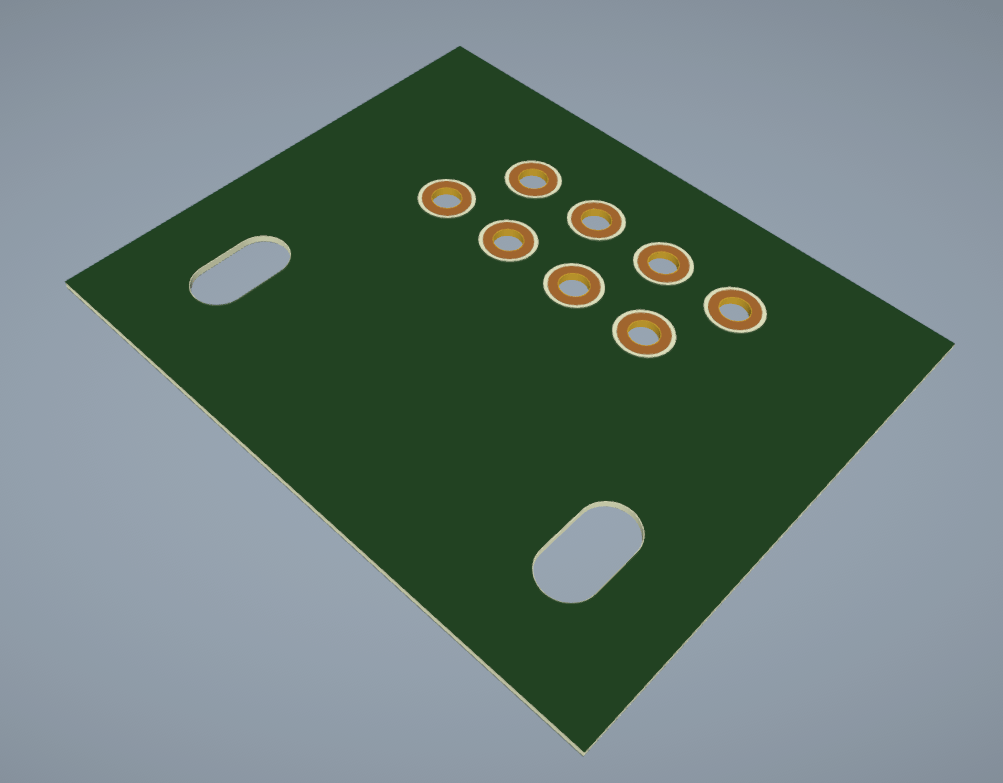
Step 18: View the footprint rendering. Both non-plated slots are shown at the bottom of the footprint.
Note: The footprint is saved in the working directory as ss-7188v-a-nf_slot.pad and can be reused in any design.
Wrap Up & Next Steps
Quickly add slots to a PCB footprint to adhere to the functional and mechanical requirements of your components and PCB designs with OrCAD X Presto. To test this feature and more, get a free trial of OrCAD and start building. Want to learn more about OrCAD X Presto? Check out our other how-tos and step-by-step walk-throughs at EMA Academy.

